


Contents
Stacked vias are considered the most suitable solution for manufacturing HDI boards with advanced features. The configuration, with microvias positioned one above another, not only leaves more room for routing but also reduces the parasitic capacitance in your PCB design.
In this case study, we will tell you about the challenges that we faced while designing 8- and 14-layer high-density boards with stacked microvias and how we solved them without compromising the design or manufacturing standards.
Case 1: 8-layer HDI board design specifications

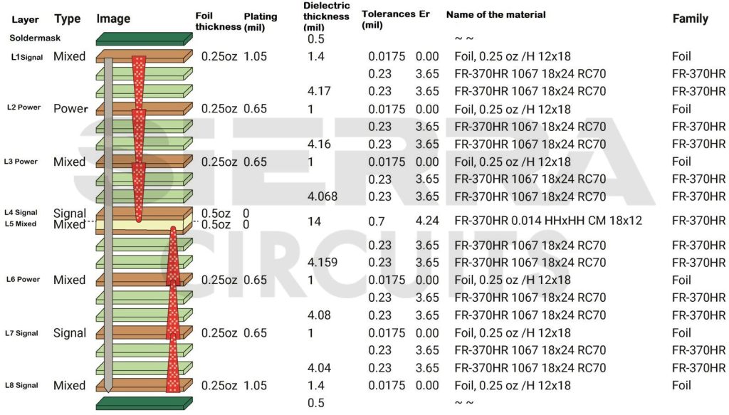
- This is an 8-layer HDI PCB with a 48 mil total thickness.
- The copper thicknesses of the inner and outer layers are 0.7 mil (0.5 oz) and 1.4 mil (1 oz finished thickness), respectively.
- The design requires controlled impedance traces.
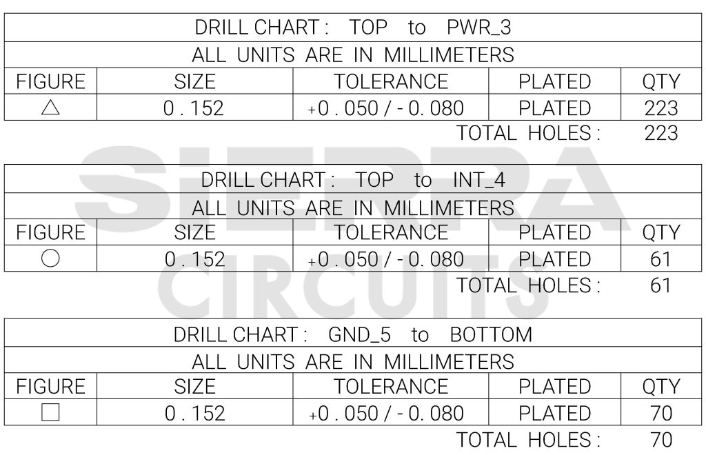
- Blind vias exist from:
- Layers 1 to 3
- Layers 1 to 4
- Layers 5 to 8
- The diameter and aspect ratio of the blind vias are 6 mil (0.152 mm) and 0.8, respectively with a tolerance of +2 mil and -3.14 mil.
- The minimum line width and spacing required is 3.3 mil.
- The thickness of the dielectric layer is 5 mil.

Tool features:
- Uses the 2D numerical solution of Maxwell’s equations for PCB transmission lines
- Supports 82 impedance models based on the trace geometry and the relevant reference planes
- Calculates the optimum trace width for a given impedance value
- Determines total insertion, dielectric, and conductor losses
Manufacturing constraints of 8-layer HDI circuit board
- The dielectric thickness and drill sizes were 5 mil and 6 mil, respectively. Achieving a 0.8 aspect ratio for these dimensions with controlled depth drilling was challenging.
- To meet the desired aspect ratio:
- The drill sizes could not be increased as the design had tight space constraints.
- The dielectric thickness could not be reduced as that would violate the controlled impedance requirements.

HDI PCB Design Guide
5 Chapters - 52 Pages - 60 Minute ReadWhat's Inside:
- Planning your stack-up and microvia structure
- Choosing the right materials
- Signal integrity and controlled impedance in HDI
- Manufacturing considerations for higher yields
Download Now
Techniques that we implemented to solve manufacturing issues
- The blind vias were split in the following manner to reduce the span and achieve a controlled depth drill:
- Blind via from layers 1-3 ⇒ split into 1-2 and 2-3
- Blind via from layers 1-4 ⇒ split into 1-2, 2-3, and 3-4
- Blind via from layers 5-8 ⇒ split into 5-6, 6-7, and 7-8
- Filled microvias were used to ensure a reliable electrical connection.
- The dielectric thickness was reduced to 4 mil to achieve the target impedance and the required aspect ratio.
Case 2: 14-layer HDI board design specifications
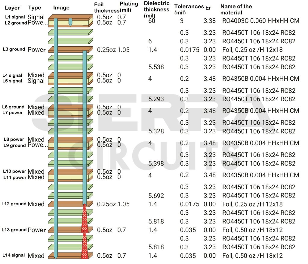
- The stack-up has 14 layers with a total thickness of 138 mil.
- The design involves blind via from layers 1 to 2, layers 3 to 14, and layers 13 to 14.
- The minimum line width and spacing is 3 mil.
- The copper thickness requirements for different layers are as follows:
- 2 mil (1.5 oz) for the top layer
- 2.6 mil (2 oz) for the bottom layer
- 2 mil (1.5 oz) for inner layers 3 and 12
- 1.37 mil (1.0 oz) for the rest of the inner layers
- An RF signal connects layer 1 and is referenced at layer 2. Hence, the dielectric thickness between layers 1 and 2 is set to 60 mil despite the fact that this results in an unbalanced stack-up.

Tool features:
- Includes a library of single and sequential lamination stack-up templates
- Offers 3 technology levels (level I/II/III) with respect to trace geometry, drill sizes, spacing, and cost index
- Automatically chooses the construction type(foil or core)
- Linked to our 2D field solver-based impedance calculator to design high-speed traces
Challenges involved in fabricating 14-layer HDI
- Due to the 60 mil dielectric thickness, having a blind via between layers 1 and 2 with a 0.8 aspect ratio was a tedious task.
- Drilling a blind via between layers 3 to 14 appeared difficult since there was a core construction present between them.
- It was critical to fulfilling the specified copper thickness requirements with 3 mil spacing.

RF & Microwave Design Guide
8 Chapters - 44 Pages - 60 Minute ReadWhat's Inside:
- Basics of RF and microwave board design
- Choosing RF materials
- Trace, grounding, via, and stack-up design
- Component selection and placement
- Testing and isolation requirements to avoid interference
Download Now
How we resolved the fabrication issues
- To achieve the desired aspect ratio, the following techniques were incorporated:
- Blind vias lying between layers 3 and 14 were split to blind via layers 3-12 and layers 12-13.
- After the final lamination, a microvia from layers 13 to 14 was drilled.
- A microvia was included between layers 1 and 2 and processed as a subset with 60 mil dielectric thickness. This sub-board was then laminated to layer 3-14 construction. All the vias were filled and stacked.
- The core construction between layers 3–14 was changed to foil construction.
- The copper thickness was modified to 0.7 mil (0.5 oz) for the inner layers and for the outer layers to 1.4 mil (1 oz).
Our DFM engineers examined and optimized the controlled impedance, aspect ratio, dielectric thickness, and via drill sizes to ensure no errors would arise later in the manufacturing process.
We have expertise in constructing complex HDI, high-speed, and high-voltage PCBs. Let us know in the comments section if you have any queries about designing reliable high-density boards. We will be happy to help you.
About Poulomi Ghosh : Poulomi is a microwave engineer specializing in EMI, EMC, RF, and high-speed electronics. As a senior technical writer at Sierra Circuits, she creates advanced engineering articles and webinars for hardware engineers and PCB designers.


