


Contents
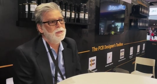
The power integrity expert, Steve Sandler of Picotest, shared his perception about power integrity in PDN design, S-parameters, and Picotest Bode 100 vector network analyzer with us during DesignCon 2022. Watch the full video here.
The power integrity expert, Steve Sandler is the founder of Picotest, a company that specializes in power integrity solutions including measurement products, services, and training. He is an expert in the design, measurement, modeling, and simulation of power, PDN, and lumped element RF circuits.
What are the best ways to determine the dynamic current required for calculating target impedance for a PDN design?
Steve Sandler: Well, it is a hard question. I gave two papers on it here at DesignCon this year, and there is not an easy way. Last year, Heidi Barnes and I gave a paper on how to make measurements from a VRM and board to determine what the dynamic current is. It is a lot of work and not perfect. The best way probably is the designers’ tools. Almost every designer provides a tool for calculating dynamic current. Again, it is not perfect. Then the least accurate is just the rule of thumb that was provided by Larry Smith, who invented target impedance. It is that you take the maximum operating load current and divide it by two, take the delta voltage allowed and divide it by the delta current allowed and it will give you the target impedance.

How do you design a PCB for optimal power integrity?
Steve Sandler: That is a tricky question. There is always this trade-off between signal integrity and power integrity. Adding to the complexity is how many I/O signals, and how many data signals come out of the I/O because the chip is pretty vague and most of the balls are allocated to signal channels. Of course, the signal integrity engineers want all of the board space to be allocated to them, and the power engineers expect the same. Typically, the way it works is that we allocate two sides to power and two sides to signal. That gets a lot more difficult with bigger chips. I spoke to two manufacturers here and we have a couple of customers of our own that have more than a thousand amperes going to a single signal. So the printed circuit board is getting a lot more challenging from the power integrity perspective, but it is always a kind of a negotiated point.

Signal Integrity eBook
6 Chapters - 53 Pages - 60 Minute ReadWhat's Inside:
- Impedance discontinuities
- Crosstalk
- Reflections, ringing, overshoot and undershoot
- Via stubs
Download Now
How are the bulk capacitors selected for better power integrity?
Steve Sandler: Based on the design of the printed circuit board, we end up with an inductance in the power plane, and we have a lot of control over the thinner dielectrics. Thinner dielectric layers mean lower inductance. But however, we have designed with some distance between the voltage regulators, and the power chip, and some thickness of the dielectric results in some inductance from the power planes. Then we have to determine the bulk capacitors from that inductance on the target impedance. The bulk capacitance is equal to the plane inductance divided by the target impedance squared. That tells us a couple of things. One is that we do not want the impedance to be as low as possible because that makes the capacitors as big as possible to second order. This number is getting big fast. What we want to do is minimize the plane inductance, and then we calculate the bulk capacitance for C=L/R2. We try to set the bulk capacitor ESR to be equal to the targeted vehicles.
What are the best practices for decoupling capacitor selection and optimization to achieve target impedance in PDN design?
Steve Sandler: You don’t select the decoupling capacitors any differently than the bulk capacitors. The ideal goal is to have a flat impedance. The capacitance is equal to inductance divided by resistance squared ( C=L/R2 ). The resistance is the target impedance. Presumably, we know what the target impedance is so we select the decoupling capacitors to be equal to the inductance divided by resistance squared. Now, where to put them, that is a whole different story. Most simulators today have optimizers built-in that will figure out where the ideal placement is. But, we do know what the total capacitance is from that C=L/R2. We know what to do with that. If you can get the package impedance, and the actual characters, the impedance of the chip package, then you could set the target impedance to be equal to that. And then again, set it C=L/R2. Very clearly everything is revolving around what the target impedance is and how much plane inductance we got.
See 4 common PDN design challenges and how to resolve them to learn about power distribution network design.
Poor control loop stability results in degraded power supply rejection ratio, transient response, and degraded jitter for mixed-signal circuits. What is the best way to design stable control loops?
Steve Sandler: Interestingly, a power supply looks a lot like a printed circuit board plane. It is inductive because of the control loop. In a very simplistic way, we can stabilize the power supply the same way we control resonances in the board by setting the capacitance C=L/R2. If we can set the resistance of the power plane to our target impedance and we know the inductance of our voltage regulator, we can select the appropriate capacitors. We also have to pick both capacitors, bulk. and decoupling, based on the board inductance. A lot of the capacitors that we place are not for the regulator, but the power distribution network. At the same time, the stability of the power supply is a function of those capacitors. Now we have to solve two different equations at the same time. One is to get the right amount of capacitance for the board, and one is to make it match the voltage regulators so the voltage regulator is stable. It gets a little bit tricky, but that is essentially how we do it.
Can you tell us some important facts about dielectric absorption that is the cause of transmission line losses? What can you do to reduce its impact?
Steve Sandler: The loss is both a good thing and a bad thing. It means in our high-speed boards, that we are losing the signal as we travel across the board. It degrades the core of the signal. But the absorption reduces the resonant Q of our circuit board. In some ways, we like the absorption loss too. It is kind of a balancing act, but we can reduce it in two ways. One way is to use lower loss materials, right on almost all of the dielectric manufacturers opt for very low absorption board materials for RF or microwave. But another tip is that if we can make the layers thinner and the traces narrower, we also end up with a higher loss. Conversely making thicker dielectrics and wider traces reduces the loss.

High-Speed PCB Design Guide
8 Chapters - 115 Pages - 150 Minute ReadWhat's Inside:
- Explanations of signal integrity issues
- Understanding transmission lines and controlled impedance
- Selection process of high-speed PCB materials
- High-speed layout guidelines
Download Now
S-parameters play a crucial role in high-speed simulations. What makes them so important?
Steve Sandler: If we go back far enough, why did they invent S-parameters? I am not even sure who invented them. I think it was Hewlett-Packard in the late Jurassic era, somewhere around there. But they were trying to make measurements and realized that no matter how they tried, the probes were always in the way. They could never make probes that were good, high enough bandwidth. Then, they came up with this methodology that said, “Well, if we matched all signals to some impedance. The signal generators are 50-ohms and we also make coaxial cables through 50-ohms.” Somebody realized if we make all of our measurements with 50-ohm sources and 50-ohm terminators, then they perfectly match the cable and the bandwidth becomes essentially unlimited.
We can make very high-frequency measurements if we match those cables and instruments. And so if, we end up with what we now call scattered parameters. It means connecting these 50-ohm ports to all of our dots and measuring transmissions and reflections of everything connected to 50-ohms. Then we can transform that to impedance, that is what we want most of the time. But the reason we do the S-parameters in the first place is that we get very high bandwidth measurements without probes being in the well.
The Picotest Bode 100 Vector Network Analyzer measures the stability of control circuits, power-plane impedance, parasitics, etc. Can you tell us some more features crucial for PCB testing?
Steve Sandler: The Bode 100 Vector Network Analyzer with a hundred analyzers is kind of unique. I think there is probably only one other analyzer that has this feature, but it can do both vector network analysis of frequency response, and also S-parameters. Those are different. We said the S-parameters being that we are making 50-ohm measurements of transmissions, reflections, and frequency response analysis. Here, we use three ports, one degenerator signal, and then use one to measure voltage, one to measure current, and divide voltage over current. That tells us impedance also. The Bode 100 allows us to measure the excess inductance and the capacitance of power planes and even vias. It measures frequency response, which is power supply rejection ratio control loop gain. We can even reconfigure that to measure S-parameters with the frequency response analyzer.
On the S-parameter side, we can use it for everything that a vector network analyzer would be used for. A lot of people use them for tuning antennas. So, if you are one of those old-timers who still has a CB radio, Bode 100 will help you tune your antenna. I can’t leave this out because the very first time I saw a Bode 100, I talked to the manufacturer about what they use them for. They said it was for measuring the ripeness of fruit. And I said, “What?” And they said, “Yes. We use Bode 100 to measure impedance.” Grocers use impedance to determine the ripeness of their fruit, and health companies use Bode 100s to measure the impedance of blood plasma. To be honest with you, the very first Bode 100 we sold was to the National Institute of Health to measure blood plasma.

The Picotest probe measures impedance, step load, ripple, etc. What makes them superior to various active and passive probes?
Steve Sandler: They are perfectly matched and set to specific pitches that match the common pitches placed on printed circuit boards. They are easy and fast to use because of their browser probes and high bandwidth.
Any interesting new Picotest product releases this year?
Steve Sandler: We are showing a few here at Tektronix that are a little early. They are not ready to be released yet. But we do have a new set of adapters for oscilloscopes that allow us to measure two-port PDN and impedance in the oscilloscope. We are showing those off, and also introducing the latest version of our differential time domain reflectometer to USB sticks, ten and a half GHz into USB sticks. We also have a couple of new probes coming this year, and those are also at the Tektronix booth today.
What is the latest trend in the power integrity world?
Steve Sandler: I have to say wide-bandgap followed probably by wide-bandgap. Wide-bandgap has been coming for 10 years, at least. So the slowest moving tidal wave, I think I’ve ever seen. But it is finally here and transforming the world of electronics in a big way. Analog and power engineers used to use low-speed and all of a sudden they have power switches that are gigahertz switching. You put that onto a printed circuit board and all of a sudden ground out of Vdd droop and plain inductance, it takes on all new meanings. We wish we didn’t see it because it is not always a pretty sight. It means that we have to be much more careful about how we design printed circuit boards to achieve wide-bandgap stability.
We become more sensitive to things like semiconductor bond wires. Those bond wire parasitic conductance combined with the board at very high frequencies to resonate and even the printed circuit board itself. It is very easy to destabilize a gallium nitride element just from a printed circuit board without adding anything else. There are some great videos about that. One of the most fascinating is by one of my superheroes Matt Ozalas in Keysight. He did this analysis of the gallium nitride transition, why it was unstable on a printed circuit board, and how important it was to fix it. He looked at the board, and simulated the board, added a via. It is fixed.
And we said, “What?” He had this video, it is the most incredible thing. I think that the takeaway from that is we always thought, at least in the power world, that the printed circuit board was just there and it just makes these connections. We did not have to worry about it. But now, even power electronic engineers have to be aware of the impact of the printed circuit board on their design, and how to optimize the design through the printed circuit boards. The printed circuit board is a very essential element and it is the one that we need to optimize. So I think gallium nitride and wide-bandgap, in general, are changing the world in that way.
About Poulomi Ghosh : Poulomi is a microwave engineer specializing in EMI, EMC, RF, and high-speed electronics. As a senior technical writer at Sierra Circuits, she creates advanced engineering articles and webinars for hardware engineers and PCB designers.


