


Contents

On-demand webinar
How Good is My Shield? An Introduction to Transfer Impedance and Shielding Effectiveness
by Karen Burnham
Electromagnetic interference (EMI) is mainly caused by poor field containment. You can reduce it by designing a stack-up with solid reference planes, minimizing loop areas, and applying filter circuits near noise-prone sections.
PCB designers and electrical engineers must first identify the source of interference and incorporate appropriate layout methods to prevent it.
To achieve electromagnetic compatibility (EMC) on the first attempt, you must understand how electromagnetic fields are generated, contained, and coupled on a board.
In this article, you will learn how interference occurs, the typical noise sources, and 7 PCB design guidelines for EMI and EMC.
Highlights:
To avoid EM interference in your circuit boards:
- Build a stack-up with solid, adjacent reference planes for every signal layer.
- Avoid routing sensitive traces near board edges and minimize trace length and loop area.
- Never leave traces, test points, or unused IC pins floating, as they act as antennas.
- Employ decoupling capacitors and EMI filters at noisy entry and exit points, and use shielded enclosures to contain conducted and radiated interference.
What is EMI in PCBs?
Electromagnetic interference happens when electromagnetic energy from one device disrupts another device’s operation. This energy can travel through the air (radiation) or through wires and cables (conduction).
EMI problems most commonly occur between 9 kHz and 6 GHz. This guide focuses on that frequency range. Above 6 GHz, interference usually stays within a single board or PCBA. These higher-frequency problems are usually considered signal integrity issues rather than strictly EMI, which more commonly deals with interactions between different systems or different parts of a larger system.
How EMI spreads
EMI occurs when electromagnetic fields interact with electronic components in unwanted ways. Fields can be created on a PCB and then:
- Radiate directly into the air (radiated emissions)
- Couple into wires and affect other components (conducted emissions)
External electromagnetic fields can also enter your system:
- Through the air, affecting PCB traces or wiring directly (radiated immunity or radiated susceptibility)
- Through shared power lines or cables (conducted immunity or conducted susceptibility)

EMI cannot be eliminated. However, we can design electronics to:
- Be less vulnerable to EMI from other sources
- Generate less EMI that affects other devices
This is called achieving electromagnetic compatibility (EMC).
What is EMC?
Electromagnetic compatibility is the ability of a printed board to operate correctly in an EM environment without being affected by external noise and without disturbing nearby circuits.
A design is considered electromagnetically compatible when it keeps its emissions low and remains resistant to external noise, in accordance with the regulatory standards.
A good EMC design makes sure switching signals follow controlled current return paths, high-frequency energy is contained, and noise doesn’t interfere with nearby circuits.
Download the High-Speed PCB Design Guide for more on layout techniques.

High-Speed PCB Design Guide
8 Chapters - 115 Pages - 150 Minute ReadWhat's Inside:
- Explanations of signal integrity issues
- Understanding transmission lines and controlled impedance
- Selection process of high-speed PCB materials
- High-speed layout guidelines
Download Now
What are the sources of electromagnetic interference?
Electromagnetic interference originates from any component or layout feature that creates rapidly changing currents or voltages.
The common sources of EMI are listed in the table below.
| EMI source | How these sources produce EMI |
|---|---|
| Digital clocks, switching ICs, SMPS, DC–DC converters | Fast rise and fall times generate high-frequency harmonics that radiate or conduct through power and signal paths. |
| LED drivers, motor controllers, and power control circuits | Rapid on/off switching produces broadband emissions and increases noise. |
| Brushed/brushless DC motors, AC motors | Arcing, commutation, and magnetic field changes create broadband noise. |
| Unshielded or unterminated cables | When the cable length approaches a quarter wavelength (λ/4), it becomes resonant and radiates harmonic frequencies. |
| Ribbon cables with poor ground distribution | Overlapping EM fields and shared return paths increase crosstalk and radiation. |
| Long, unterminated, high-speed signals | When the trace length approaches λ/4 of a harmonic, it radiates like an antenna. |
| Floating heat sinks, metal frames, and brackets | Metal objects act as an antenna if not connected to a reference plane. |
| Large signal or power loops, poor return path placement | Increased loop area strengthens magnetic fields and raises radiated emissions. |
| Gaps in planes, enclosure holes, panel seams | When the slot diameter approaches λ/2, they behave as slot antennas and radiate strongly. |
| Improper shield contact | Bonds with high impedance prevent effective shielding, especially at high frequencies. |
| 4-layer boards without adjacent reference planes | Poor field containment forces return currents to take longer paths, increasing loop area and noise. |
| Split planes, gaps, and long detours for the return current | Increases loop area and radiated EMI. |
| Missing or poorly placed decoupling capacitors | High-frequency noise appears on power rails, increasing interference. |
| Unused MCU pins, unconnected traces, test pads | Floating conductors act as antennas. |
Understanding where interference originates is the first step in preventing it. In the next section, you’ll learn the PCB design guidelines for EMI and EMC that help you contain fields efficiently.
To avoid common layout mistakes that lead to EMI failures, see PCB layout rules every designer should follow.
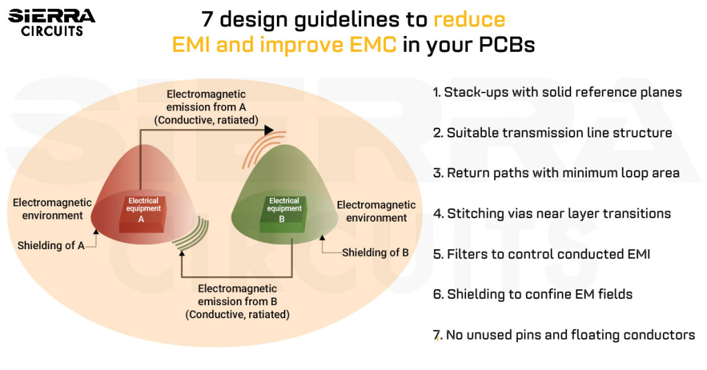
7 design guidelines to reduce EMI and improve EMC in your PCBs
To achieve electromagnetic compatibility, your design must contain EM fields, provide uninterrupted return paths, suppress noise at its source, and prevent interference from escaping through traces, vias, cables, or enclosures.
These circuit board design guidelines for EMI and EMC cover stack-up design, controlled routing, return-path management, via transitions, filtering, and shielding to reduce interference and improve compatibility.
1. Build a stack-up with solid reference planes
A well-planned circuit board stack-up is the foundation for passing EMC testing on the first attempt. It provides the necessary reference planes needed to contain fields and ensure clear return paths.
Stick to these guidelines to ensure a low-noise design:
- Provide an adjacent reference plane for every signal layer. Any layer carrying switching signals or high-speed traces must have a solid ground or power plane immediately next to it (above or below). This pairing creates a controlled-impedance structure and confines the signal’s EM fields, preventing radiation.
- For instance, in a standard multilayer board, the top layer (layer 1) contains components and traces that usually generate noise. A continuous ground plane on layer 2 provides an immediate, low-inductance return path directly beneath the signal layer. Fields are contained between layer 1 and layer 2.
- Prefer a 6-layer (or higher) stack-up for robust EMC performance. A recommended arrangement is shown below. This ensures every signal layer has an adjacent ground plane.

Preferred 6-layer stack-up to avoid EMI. - If you’re implementing a 4-layer stack-up, consider the example below. The preferred stack-up is: L1: signal; L2: ground; L3: power; L4: signals.

Preferred 4-layer stack-up to avoid EMI (left). A layer stack-up with no adjacent plane and very little field containment on layer 4 (right). - Use grounded copper pours on outer layers with stitching vias. Adding ground floods (copper pours) to the top and bottom layers can enhance field containment. However, they are only effective and safe if they are heavily stitched with multiple vias to the internal ground plane(s). A floating or poorly connected copper pour can act as an antenna and worsen EMI.
- If your stack-up requires a signal layer without a nearby ground or power plane (which should generally be avoided), you must intentionally control the return path. Route signals as tightly coupled signal-and-return pairs and use techniques such as guard traces if necessary, to keep electromagnetic fields contained.

2. Choose the right transmission line structure
One of the biggest challenges in high-speed boards is preventing trace noise from radiating as EMI.

Apply these PCB design guidelines for EMI and EMC:
- Choose an appropriate transmission line structure (microstrip or stripline, or two-wire transmission line) for all high-speed signals.
- For exceptionally noisy (e.g., clocks) or highly sensitive (e.g., analog) traces, use a stripline configuration, in which the trace is sandwiched between two solid reference planes. This offers the tightest field confinement and best isolation from other layers.

Stripline PCB transmission line structure. - Use microstrip for general-purpose routing. For most digital signals, I/O, and power routing, a surface trace over an adjacent reference plane (microstrip) provides sufficient field containment and is easier to implement and debug.

Microstrip PCB transmission line. - Don’t split ground planes. Always use a single continuous reference plane.

Do not split ground planes. - Manually create return paths on single-layer boards without an internal ground plane. Route the signal trace immediately adjacent to its dedicated return trace to form a two-wire transmission line.
- Place guard traces on both sides of the signal to reduce field spreading. In multilayer PCBs, guard traces must be stitched to the adjacent reference plane using multiple vias to maintain a low-impedance ground connection. On single-layer boards or layers without a reference plane, guard traces can only be grounded at their ends and offer minimal EMC improvement.

Guard traces confine EM fields.
- Place guard traces on both sides of the signal to reduce field spreading. In multilayer PCBs, guard traces must be stitched to the adjacent reference plane using multiple vias to maintain a low-impedance ground connection. On single-layer boards or layers without a reference plane, guard traces can only be grounded at their ends and offer minimal EMC improvement.
For more, see 10 best high-speed PCB routing practices.
3. Implement return paths with minimum loop area
Uncontrolled return paths are a major source of EMI. Every signal forms a loop with its return path, and the larger that loop, the more efficiently it radiates.
By keeping return paths tight and minimizing loop area, you can significantly reduce unintended emissions and avoid common EMC failures.
Implement these layout rules to reduce loop areas:
- Keep all traces and components away from the board edge.
- Maintain a distance of at least one dielectric thickness (the height from the trace layer to its reference plane).
- Minimize trace lengths, especially for critical signals. Shorter traces reduce the physical antenna size, decrease loop area, lower impedance, and improve signal integrity. Apply this rule aggressively to clocks, high-speed digital lines, and switching power supply nodes (e.g., PWM signals) to limit their radiation potential.
4. Add stitching vias near layer transitions
When a signal changes layers through vias, its return path can become discontinuous, allowing electromagnetic fields to escape and radiate. Adding stitching vias around signal transitions preserves return-path continuity, maintains controlled impedance, and minimizes EMI.
Implement the following PCB design guidelines for EMI and EMC when designing vias:
- Add ground-stitching vias adjacent to any signal via transitioning between layers to maintain a continuous return path and keep electromagnetic fields tightly confined around the via structure. Ensure the ground vias connect to the correct reference plane so the return current flows smoothly before and after the transition.

Place stitching vias when a signal changes its ground reference. - Skip stitching vias when the signal transitions through a hole that passes entirely through a solid, uninterrupted reference plane (e.g., layer-1 → layer-3 with a continuous ground plane on layer-2). The ground plane on layer 2 provides the return path when no reference-plane discontinuity exists.

A via transitioning through a continuous ground plane does not require stitching vias, as the plane provides an uninterrupted return path for the signal. - Use via fences along the PCB edges to form a vertical grounding wall that ties ground layers together and confines high-frequency fields. This reduces edge radiation, especially where sensitive or noisy signals run near the perimeter.

A Faraday cage restricts the emission/interference within the defined area of a PCB. - Set via-to-via spacing to less than λ/20 of the highest frequency of concern to ensure the via fence acts as an effective EMI barrier.
- For example, if your highest problem frequency is 1 GHz (wavelength = 18 cm in FR4 material). λ/20 = 0.9 cm. Therefore, via fence spacing should be less than 9 mm.
For more, download the PCB Via Design Guide.

PCB Via Design Guide
7 Chapters - 90 Pages - 70 Minute ReadWhat's Inside:
- Guidelines for choosing the right via for your application
- Design rules for advanced via structures
- DFM tips to avoid manufacturing errors
- Signal integrity considerations for high-speed designs
- Testing and inspection methods for via reliability
- Fab notes
Download Now
5. Apply filters to control conducted EMI
Filters control high-frequency noise on power and signal lines to prevent it from coupling into sensitive circuits or radiating via cables and apertures. Without filtering circuits, noise can escape your system or enter it through conductive paths, turning I/O lines into unintentional antennas.
Apply these filtering methods to prevent noise from coupling into cables and interfaces:
- Place decoupling capacitors as close as possible to the IC’s power and ground pins (preferably in millimeters) to minimize loop inductance. Connect them directly to a solid ground plane and keep the power →capacitor → ground loop as small as possible. A large loop acts like a radiator; a tight loop suppresses noise at the source.

A decoupling capacitor connected to a power source. - Install EMI filters at all entry/exit points of power inputs, I/O connectors, and communication ports. Filtering before signals reach cables ensures internal noise doesn’t escape and external noise doesn’t enter. Cables without filtering become efficient antennas for high-frequency noise.
- Choose passive EMI filters (LC, π, or C-filters) based on required attenuation, frequency range, current handling, board space, and cost. Active filters are rarely needed in most digital/embedded designs, and passive solutions are simpler and more robust.
If filtering alone doesn’t solve radiated interference, combine it with shielding. Filters block conducted noise and shielding contains radiated fields, both of which are often needed for full compliance.
6. Implement shielding to confine EM fields
Shielding blocks electromagnetic fields by creating conductive barriers that act as Faraday cages. These barriers should be properly grounded and well sealed; otherwise, they can start behaving like antennas.
Use these shielding practices to contain emissions and protect sensitive circuitry:
- Use PCB-level shields to isolate critical circuits. Place conductive cans over noisy and sensitive areas (e.g., oscillators, switching regulators, RF receivers, and precision analog circuits) to protect them from external noise. For effectiveness, the shield must form a near-continuous enclosure with multiple low-impedance connections to the board’s ground plane.

EMI/EMC shielding can protect the signal from external noise. - For slot openings, keep hole diameters smaller than λ/20 of the highest frequency of concern, where λ is the signal wavelength in the PCB material.
- For example, if your highest problem frequency is 1 GHz (wavelength = 18 cm in FR4 material). λ/20 = 0.9 cm. Therefore, the hole diameter should be less than 9 mm.
- Implement enclosure-level shielding with a metal housing. A conductive enclosure acts as a Faraday cage, containing internal emissions and blocking external interference. For this to work, cable shields must have a 360-degree termination to the enclosure exterior, maintaining the cage’s continuity.
- Shield all cables penetrating the enclosure. Every cable passing through a conductive enclosure must either be shielded or have its signals filtered at the entry point. Unprotected cables will conduct noise in or out, defeating the shield.
- Choose a capacitive PCB-to-chassis connection in shielded enclosures. An ideal Faraday cage does not require this approach, but real-world metal enclosures often benefit from connecting the PCB ground to the chassis through capacitors at the mounting points. This provides a low-impedance path for high-frequency noise and prevents low-frequency ground loops.

PCB and chassis connection through a capacitor. - Apply PCB-level shielding for devices with plastic enclosures.
7. Terminate unused pins and eliminate floating conductors
Floating pins and unterminated traces behave like antennas, radiating internal noise and picking up external interference. These structures cause EMC failures.
To avoid this:
- Terminate all unused IC pins according to manufacturer recommendations.
- Remove leftover traces and unused test points from production layouts.

An unterminated trace on a PCB layout. - Connect all copper fills, heat sinks, shields, and metal brackets to a defined ground reference.
Eliminating floating conductors reduces unintended radiation and improves system immunity.
Sierra Circuits fabricates and assembles high-quality circuit boards that follow the stringent requirements of EMC regulatory standards.
To learn more, see our rigid PCB manufacturing capabilities.
What are the regulatory standards for testing EMI and EMC?
FCC Part 15, CISPR 11, and MIL-STD-461 define emission and immunity requirements for circuit boards.
Selecting the correct EMC standards depends on three factors:
- What type of product are you building? (consumer electronics, industrial equipment, medical devices, automotive modules, military hardware, etc)
- How and where will the product be used? (residential vs. industrial environments, portable vs. fixed equipment, proximity to sensitive systems, safety-critical applications)
- Which markets will the product be sold in? (because regulatory frameworks differ across regions such as the U.S., Europe, and Asia)
Each regulatory framework defines its own emission limits, immunity tests, and documentation rules, so a single device may need multiple certifications.
Since these requirements differ across regions and application classes, you must define them before building prototypes. Engage with an EMC test lab or consultant early in the design cycle. Clarifying the required test standards upfront will save significant time, avoid redesign cycles, and reduce certification risks.
| Standard | Scope/purpose | Key classifications |
|---|---|---|
| FCC Part 15 (U.S.) | Governs RF emissions from unlicensed electronic devices. Global equivalent: CISPR 32. |
|
| CISPR 11 (International) | Emission limits for industrial, scientific, and medical (ISM) equipment, referenced by IEC 60601-1-2 for medical devices. |
|
| MIL-STD-461 (Military/Aerospace) | Ensures military systems limit emissions and withstand harsh EMI environments; used in defense, avionics, and space. |
|
How are EMI and EMC tests performed?
Electromagnetic interference and compatibility tests are carried out by exposing a PCB to EM conditions similar to those encountered during normal operation. These tests evaluate both emissions and immunity.
Your circuit boards will be exposed to:
- Magnetic fields from electrical wires
- Radiated and conducted electromagnetic noise
- Voltage drops from power interruptions
- Fast transients from electrical switches
- Surge events that replicate lightning strikes or power grid faults
- Electrostatic discharge (ESD) from static electricity (human contact or charged surfaces)
To ensure electromagnetic compatibility of your design, build a stack-up with solid reference planes, choose a suitable transmission line structure, maintain continuous return paths with minimal loop area, and manage layer transitions using stitching vias.
Applying these PCB design guidelines for EMI and EMC early in the layout phase reduces rework and minimizes test failures.
Have queries on designing EM-compliant boards? Post them on our community, SierraConnect. Our design experts will answer them.
About Mohamed Faheemuddin : Mohamed Faheemuddin is a mechanical engineer. His passion for electronics drew him to the PCB industry. With an experience of over 3 years in the PCB industry, he specializes in developing articles for engineers and hardware designers.


Start the discussion at sierraconnect.protoexpress.com