


Contents

On-demand webinar
How Good is My Shield? An Introduction to Transfer Impedance and Shielding Effectiveness
by Karen Burnham
Designing a reliable flex PCB starts with applying the right layout techniques and selecting suitable materials to handle bending needs.
Layout engineers and hardware designers must determine the application type (static or dynamic), define the appropriate bend radius, and incorporate features such as stiffeners and flexible stack-ups to meet mechanical and electrical requirements.
In this article, you’ll learn key flex pre-layout considerations, material selection guidelines, and layout techniques to improve flexibility and manufacturability.
Highlights:
When you design a flex board:
-
- Calculate the bend radius based on the number of layers in your stack-up.
- Opt for adhesive-less flex materials for thinner laminates to avoid issues like copper plating, cracks, and moisture absorption.
- Place plated through holes at least 20 mil away from the bend area.
- Incorporate stiffeners into your design if it includes components on the flex section.
What is a flex PCB made of?
Flexible printed circuits (FPC) are built using very thin polyimide substrates. These materials offer excellent mechanical strength and thermal resistance, making them well-suited for high-temperature flex PCBs. They can also be molded into complex three-dimensional shapes for use across a diverse range of applications, such as heads-up displays for aerospace piloting and wearable technology.
These materials have an acrylic base and offer a lower dielectric constant than standard materials. The thickness of the flex PCB materials varies between 0.5 and 5 mil.
What are the applications of FPCs?
Flex boards are widely used in critical applications such as medical devices, automotive systems, and aerospace electronics, where reliability, compact design, and mechanical flexibility are essential.
- Medical electronics: Widely used in medical devices due to their compact size and 360° bendability.
- Automotive industry: Excellent resistance to vibration makes them ideal for the harsh environment inside a motor vehicle.
- Space applications: Most aerospace applications use flex boards to reduce the system’s overall weight.
For more on flex circuit board applications, see the history of flexible PCBs and their modern applications.
Why choose flex PCBs
Flex printed boards can simplify product design, reduce manufacturing costs, support both static and dynamic applications, and eliminate bulky connectors. Here are a few key reasons why designers choose them:
1. Facilitates seamless integration and enhanced functionality
With minimal design constraints, flex boards can be tailored to fit any device shape. This adaptability makes them suitable for a wide range of applications.
Additionally, they minimize the risk of potential failure points typically found in standard PCBAs by eliminating the need for connectors and extra cables. FPCs reduce the product’s overall weight and facilitate miniaturization.
2. Reduces overall board expense
Using flexible printed circuits can result in direct and indirect cost savings.
Direct cost savings
A single rigid-flex board with multiple rigid sections can replace the assembly of multiple circuit boards within a product.

For instance, if a product initially requires 6 rigid boards, a single rigid-flex PCB with 6 rigid sections can be designed to fulfill the same functionality. This consolidation eliminates the need for multiple boards, wire harnesses, and connector pairs. This inventory reduction leads to direct cost savings.
Indirect cost savings
The absence of wire harnesses simplifies the assembly process, reducing labor costs and assembly time. Since flex circuit boards can be designed to incorporate all necessary connections and wiring within the board, assembly manual components (connectors) can be eliminated. This reduces the overall cost of the flex PCB assembly process.
Wiring errors, such as incorrect connections, are common sources of product failures in standard circuit boards. Integrating wiring directly into the flex boards significantly reduces the risk of wiring errors. This improves the product’s overall reliability, leading to potential cost savings associated with warranty claims, repairs, and returns.
3. Supports static and dynamic applications
Flexible printed circuits can be used in both static and dynamic applications.
FPCs experience minimal to no bending during their operational lifespan in static applications. They are commonly found in consumer electronics like smartphones, tablets, and laptops, where they’re integrated into the device’s structure without experiencing much bending or flexing during normal use.
Conversely, dynamic applications involve circuit boards that are designed to bend during operation. They’re typically found in wearable devices, automotive systems, printers, and humanoid robotics.
4. Eliminates the requirement of bulky connectors
Traditional connectors are susceptible to mechanical wear and damage over time, especially in applications subject to vibration or movement. Hence, by eliminating these connectors, flex PCBs reduce the number of potential points of failure, resulting in improved reliability and longevity of the product.
Vern Solberg, a seasoned flex PCB expert with 25+ years in SMT and microelectronics design, explained in an interview:
“We use flex because we need a good, rugged, dependable interface. Wire cables are not always dependable, but flex is. At other times, it is because of the shape or the need to fit the product into a small space, and their flex allows us to connect two rigid boards in a very small space.”
Flex PCB pre-layout considerations recommended by Vern Solberg
Vern Solberg outlined a few tips for capitalizing on the inherent advantages of flex printed boards. Solberg holds multiple patents for IC packaging innovations, including the folded-flex 3D package technology and multiple die designs.
1. Determine the type of application
Before the layout design stage begins for your flex PCB, ensure you know the answers to the following questions:
- How many times will your PCB flex? Will it be a dynamic or static board?
- What is the bend radius?
- How thin or thick can the overall PCB be?

Stack-ups for dynamic and static devices vary, so the application and type of board must be known beforehand.
For more layout strategies, download the Flex PCB Design Guide.
Flex PCB Design Guide
10 Chapters - 39 Pages - 45 Minute ReadWhat's Inside:
- Calculating the bend radius
- Annular ring and via specifications
- Build your flex stack-up
- Controlled impedance for flex
- The fab and drawing requirements
Download Now
2. Design with your stack-up in mind
Request a stack-up from your manufacturer. It is crucial that you know how to stack your circuit board layers. Rigid-flex is the simplest configuration that will allow you to reduce the number of connectors, which will also increase wiring density and reliability.

One way to get off to a good start here and avoid rework is to build models early on, using paper or mylar. Primary components can be arranged to ensure proper fit, while rigid sections can be glued.
A face-to-face meeting with your contract manufacturer is the best way to ensure you’re on the same page regarding the overall process. This meeting can also help ensure that design guidelines and capabilities are well understood.
Sierra Circuits fabricates and assembles high-performance flex PCBs engineered to withstand harsh environments and support dynamic applications.
To learn more, see flex and rigid-flex PCB capabilities.
3. Consult your contract manufacturer
The design rules for flex and rigid-flex are different from standard rigid boards. Flex circuits require button plating, and annular rings need to be larger than rigid designs. Each contract manufacturer may have their own set of design rules and recommendations.
Always consult your manufacturer before finalizing the materials. The dielectric should be suitable for the environment and the application in which the board will operate.
4. Stick to standard flex PCB layout design guidelines
Follow the standard design rules to cut the overall board cost.
Here’s a list of IPC and mil-grade standards for flex and rigid-flex boards:
| Standards | Description |
|---|---|
| IPC-2223 | Sectional design standard for flexible/rigid-flexible printed boards |
| IPC-4202 | Flexible base dielectrics for use in flexible printed boards |
| IPC-4203 | Cover and bonding material for flexible printed circuitry |
| IPC-4204 | Flexible metal-clad dielectrics for use in the fabrication of flexible printed circuits |
| IPC-6013 | Spec for flexible/rigid-flexible printed boards |
| MIL-P-50884 | Military specification: Printed wiring board, flexible or rigid-flex |
For more, download the IPC Standards Handbook.
IPC Standards Handbook
7 Chapters - 110 Pages - 85 Minute ReadWhat's Inside:
- Clear breakdown of IPC standards for every stage of PCB development
- Design and DFM guidelines based on IPC-2221, IPC-7351, and IPC-J-STD-001
- Material selection guidance tied to IPC-4101, IPC-4202, and more
- Testing and inspection insights using IPC-A-600 and IPC-TM-650
- Best design documentation practices for seamless production
Download Now
In addition to industry standards, you need to consider the standard design practices. For instance, placing your flex layer within your rigid layers is one of the important DFM guidelines. Multilayer boards with greater complexity are in demand as pin counts rise and thousands of I/Os are incorporated into some devices.

5. Optimize your design for the specific application needs
Customize the design to align perfectly with the requirements of your application. There is no “one size fits all” approach to flex PCB layout design.
For example, exploring alternatives like rigid-flex configurations becomes necessary if your application demands more than a single-layer flex. Further, you will need to decide whether to incorporate stiffeners based on the application’s mechanical requirements, size constraints, and budget considerations.

Always know your CM’s capability. You don’t want to end up designing a board that can’t be manufactured. Suppliers have their own design rules and recommendations that should be considered.
For rigid-flex DFM guidelines, see 13 common DFM mistakes in rigid-flex PCBs and techniques to avoid them.
6. Implement modeling and testing
Creating a paper doll model before starting the prototyping process is helpful. This pre-layout consideration allows you to refine the design and layout, reducing the need for respins in your prototype. Paper doll models ensure you get your design right the first time.

Solberg explained:
“I have created a number of models simply with a piece of stiff paper, or mylar. I glue rigid and flex sections and put on the primary components. First, I ensure everything fits, and then collaborate with the supplier to choose materials that can withstand the environmental challenges ahead.”
The polyimides used in coverlay are rugged enough to handle most environments. However, issues are more common with laminates, which are less robust under harsh conditions. Laminates are unsuitable for certain chemicals or adhesives, and the vias are liable to crack without reinforcement.
The copper in flex PCBs differs from the copper in rigid boards. Flex materials also do not have glass weave or suffer from material cracking once we drill into them.
For more FPC design tips, see 7 must-knows for your first flex PCB design.
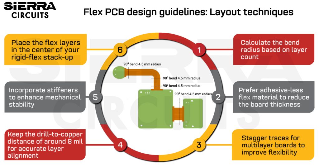
6 flex PCB layout techniques for reliable manufacturing
Flex-printed board design requires a slightly different approach than rigid PCBs. Below are a few guidelines for designing a flex board.
1. Calculate the bend radius based on layer count
The bend radius is the minimum radius up to which the flex area can bend without damage. It must be properly identified early in the design. This ensures that your design allows the necessary number of bends without damaging the copper. IPC-2223 specifies the standards for bend radius.
There are two types of FPCs:
- Static: These boards will flex less than 100 times in their lifetime. They will only flex during the installation process.
- Dynamic: These boards flex during their operation. They are typically used in printers.
The bend radius depends on the number of layers in your stack-up. You can use the table below to calculate it.
| Number of layers | Bend radius (mils/mm) |
|---|---|
| 1 (single-sided) | Flex thickness x 6 |
| 2 (double-sided) | Flex thickness x 12 |
| Multi-layer | Flex thickness x 24 |
10 tips to design reliable bend areas
- Clearly define the rigid and flex regions and the bend radius early in the design stage.

Defining rigid and flex sections - For dynamic applications, the bend radius should be 100 times the finished board thickness.
- If there are no traces in the bend region, insert circular cutouts with radii greater than 30 mil to minimize the amount of material that needs to be deformed and increase flexibility.
- Avoid plated through holes and component placement within the bend area. Place plated through holes (PTH) at least 20 mil away from the bend area.

Maintain a minimum distance of 20 mil between PTH and the bend area. - Avoid 90˚ bends as they increase the risk of circuit damage. Instead, have gradual bends that are considered safer for the circuit.

Flex board bend radius recommendations. - Place conductors smaller than 10 mil inside the neutral bend axis, where tension or compression is minimal during flexing.
- Provide sufficient space between the transition point of the flex and the rigid area from the bending point to minimize the stress on the flex layers.

The bending point is kept far away from the transition points. - Use tear guards to reinforce the flex material along the inside bend radius. This will prevent the flex material from tearing.

Tear guard along the inner bend radius to reinforce the flex material. - Maintain at least 10 mil clearance between two flex regions. With inadequate clearance, adjacent flex regions may mechanically interfere with each other, leading to bending restrictions, increased stress on the material, or even tearing.

Ensure a minimum clearance of 10 mil between adjacent flexible regions. - Use cross-hatch for ground and power planes to reduce copper on a plane layer and increase the board’s flexibility. Typically, we recommend 0.015” wide signals with 0.025” spacing for the cross-hatched plane layers.
A cross-hatch plane can be characterized by the ratio of cross-hatch conductor width (HW) to cross-hatch pitch (HP). The lesser the ratio, the greater the percentage of copper being removed.
For example, a 50% copper removal would be achieved if the ratio is about 0.293. The higher the copper percentage being removed in the cross-hatch, the higher the increase in controlled impedance compared to the solid copper plane.

2. Prefer adhesive-less flex material to reduce the overall board thickness
There are two types of flex PCB materials :
- Adhesive-based material: The copper is bonded to the polyimide with acrylic adhesive.
- Adhesive-less material: The copper is cast directly onto the polyimide.
The use of adhesives in rigid areas can create cracks in via plating. This is because acrylic adhesives become soft when heated. Consequently, when designing for adhesive-based materials, it’s important to incorporate anchors and teardrops in your design.
Drawbacks of using adhesive-based materials
- These materials are prone to absorbing moisture from the environment, making them unsuitable for use in systems exposed to the outside environment.
- The core thickness of adhesive-based material can be reduced after the fabrication process. This leads to dimensional error.
Why adhesive-less flex material is preferable
- Eliminates the adhesive bond layers and makes way for thinner laminates.
- Offers higher operating temperature ratings and higher copper peel strength.
- Moisture-resistant when exposed to the environment.
4 material selection guidelines for your flex printed circuits
- Prefer adhesive-less materials for high-speed applications due to their consistent results and cost-effectiveness. If you are choosing adhesive-based material, use acrylic adhesives of 1 mil thickness.
- If you’re mounting components on flex sections, include PCB stiffeners for mechanical support. Use Kapton when the stiffener thickness is less than 10 mil.
- Use rolled annealed copper as cladding for polyimide flex cores.

Rolled annealed copper. - FPC copper comes in 0.25oz ( 9 μm), 0.375 oz ( 12 μm), and 2 oz (70 μm). We recommend a minimum copper thickness of 0.25 oz and a maximum of 2 oz.
- The thinner the copper, the higher the flexibility.
- Select polyimide as the primary material for coverlay. It offers uniform thickness (min. 1 mil).
- Choose min coverlay thickness based on Cu thickness.
- 0.5 oz Cu or less- min. 1 mil,
- 1 oz Cu min. 1.5 mil
- 2 oz Cu min. 3 mil
- Choose min coverlay thickness based on Cu thickness.
We recommend the following materials for your flex printed circuit board:
- DuPont Pyralux AP
- DuPont Pyralux LF
- DuPont Pyralux FR

3. Stagger traces for multilayer boards to improve flexibility
6 routing strategies you should know before designing a flex circuit board
- Stagger traces when designing multi-layer flexible PCBs. Stacked traces will not only reduce the flexibility of your circuit but will also increase stress, contributing to the thinning of copper circuits at the bend radius.

Staggered and overlapping traces on flex PCB. - Keep the traces perpendicular to the bend area to eliminate the stress points that can cause trace copper breakage.

Keep the traces perpendicular to the bend area to reduce stress in the flex PCB layout design. - Avoid sharp corners in flexible areas, as they can lead to stress concentration and potential failure, especially in high-temperature flex PCBs where thermal expansion exacerbates mechanical stress. Use rounded corners instead.

Avoid sharp-edged traces to reduce stress in the flex PCB layout design. - Taper down the traces towards the end at which they are connected to the pads. This eliminates the issue where the trace entering a pad forms a weak spot, potentially causing copper fatigue over time.

Tapering the pads where traces enter resolves weak spot concerns. - Do not include via-in-pad in flex designs, as it can damage the thin substrate during planarization. Moreover, the smaller aspect ratio of the vias does not allow non-conductive epoxy filling, and it can hamper the electrical conductivity of the vias.
- Implement additional through-hole plating of up to 1.5 mil to provide mechanical support from one flex layer to another.

Additional plating, anchored stubs, and reduced coverlay access openings for PTH mechanical support in the flex board. For advanced applications such as humanoid robotics PCBs, ultra-thin flexible substrates allow engineers to develop highly maneuverable robotic components without compromising electronic performance.
4. Maintain a minimum 8 mil drill-to-copper distance for accurate layer alignment
9 ways to design reliable vias on flex boards
- Teardrop annular ring when dealing with traces thinner than 20 mil to enhance the board’s structural integrity against shear force and vibrations.
- Incorporate anchors and spurs encapsulated with coverlay to avoid trace lifting and pad peeling.
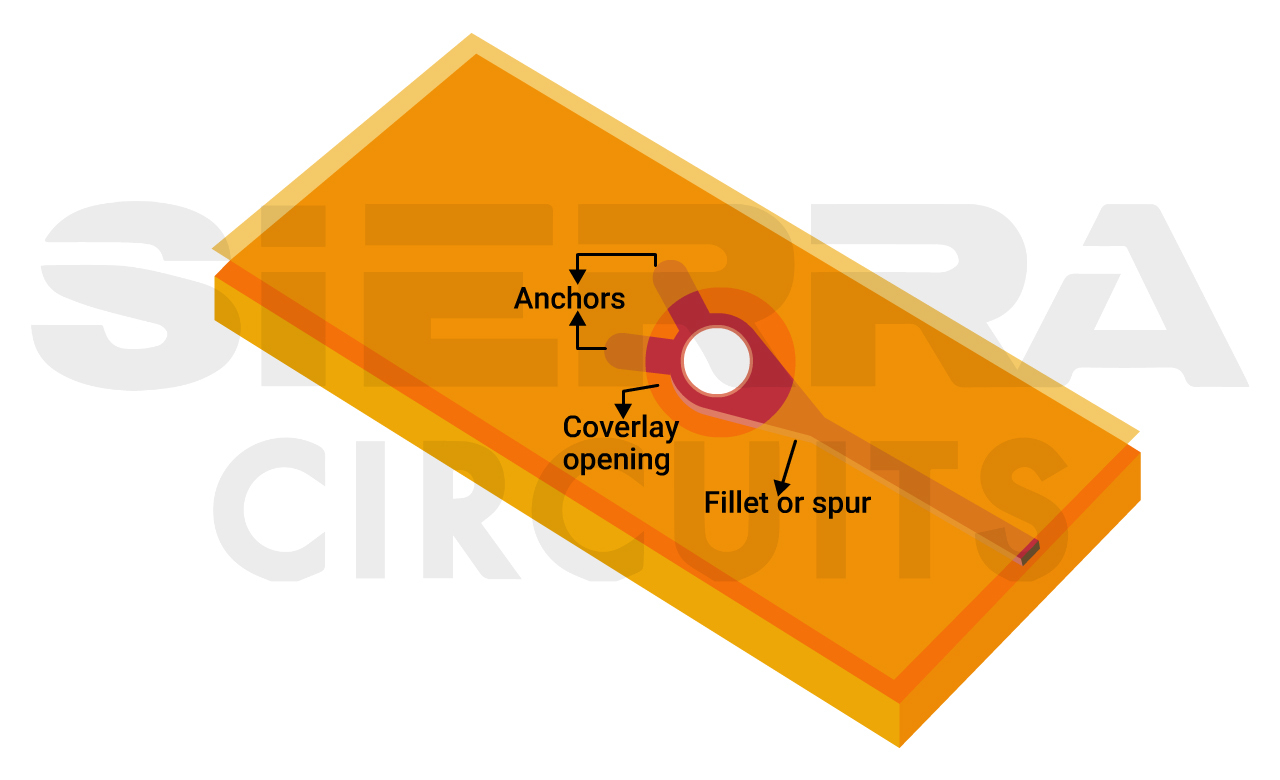
Anchors and fillets on FPC traces and pads. - Avoid vias in the flex section of dynamic boards, as they are at risk of cracking.
- Maintain at least 50 mil space between the vias and the stiffener’s edge. Vias are safe over a stiffener, but those placed just off its edge risk cracking.
- Place vias at least 30 mil away from the rigid-flex/flex interface.
- Maintain a hole-to-flex distance of 50 mil to increase the board’s reliability. This distance can be reduced to 30 mil for commercial applications. Insufficient clearance can generate undesired stress during bending and detach the via from its plating.
- Prefer pad-only plating (button plating) for flex boards. In this process, copper is deposited only on the vias/pads, reducing the amount of copper, which increases the board’s flexibility. Further, it aids in improving etch yields in small etch patterns by allowing manufacturers to control the copper thickness. However, the extra processing steps make this expensive.
- Keep the drill-to-copper distance of around 8 mil to achieve accuracy in layer alignment. This aids in the manufacturing process as flex materials are prone to more movement and contraction.

Maintain at least 8 mil spacing between the drill and the copper in the flex PCB layout design. - Keep the annular rings as large as possible (at least >8 mil) to improve the mechanical strength of the connection.
5. Incorporate stiffeners to enhance mechanical stability
The stiffener is an additional mechanical piece that provides mechanical support to your PCBA. By adding localized rigid material, single-sided, double-sided, and multilayered flex boards can be stiffened in specific areas.
When you add stiffeners, ensure they overlap the coverlay by 30 mil as shown below.

6. Place the flex layers in the center of your rigid-flex stack-up
Request a stack-up from your manufacturer in the design phase. You must know what stack-up you are designing. Rigid-flex is the simplest configuration that will allow you to reduce the number of connectors, which will also increase wiring density and reliability.
Having a face-to-face meeting with the supplier is the best way to ensure that you’re on the same page in terms of where the overall PCB process is headed. This meeting can also help ensure that flex PCB layout design techniques and capabilities are well understood.
Also, see flex PCB assembly for bendable board manufacturing and rigid-flex assembly for hybrid designs that combine stability with flexibility.
6 design tips to build flex and rigid-flex stack-up
- Position the flex layers in the stack-up’s center to protect from exposure to outer-layer plating. This placement also simplifies manufacturing and improves impedance and control in the flex area.
- Use an even number of layers to ensure a balanced stack-up.
- Utilize CAD tools for virtual mock-ups during the early design phase. You can create flex board models using stiff paper or Mylar.
- Provide impedance trace details such as trace width, height, and impedance tolerance in the stack-up.
- Use bookbinding in rigid-flex boards, allowing more flex layers to navigate tight bends without deformation. It allows the PCB to perform bends of 180˚ or more. However, a board with bookbinding costs 30% more than a standard rigid-flex one.

Bookbinding construction in rigid-flex PCB. - Implement the rigid-flex air-gap construction method to eliminate the flex adhesives within the rigid sections. This method also addresses the via reliability issues and improves bendability.

This was a four-layer flex board with zero insertion force (ZIF) connectors requiring controlled impedance.
This stack-up had a few issues. First, the board’s flex layers were located on the top of the stack-up, which increased the risk of potential manufacturing issues. When the flex layers are on top, the panels are harder to handle and process.
We embedded the flex layers in the center of the stack-up, as shown below.

This protected the layers during manufacturing and ensured that the less-durable flex layers were not exposed to outer-layer plating. Further, this arrangement made the board more durable and easier to manufacture.
Our surface plating also protects the flex layers. Rigid AP material was used, allowing for better impedance control. It was a much better option than the original FR-4 material.
In some cases, you might not have the original design files, especially when working with legacy hardware. This can pose a significant hurdle for manufacturing new flex PCBs. The case study, reverse-engineering a flex PCB to generate design files, showcases how reverse engineering can be a successful solution in such scenarios.
For customized solutions tailored to your specific needs, partner with us.
You can book a meeting with our experts or call us at +1 (800) 763-7503.

What to include in your flex PCB fab drawings
To successfully design a flexible PCB, you need to have a basic understanding of the fab drawing requirements, which include:
- Flex board stack-up construction and layer order
- Dimensional drawing and tolerances
- FPC materials to be used
- IPC class type (class 1,2, or 3)
- Drill symbol chart
- Bend radius
- Plating and marking requirements
- Flex PCB testing standards
Fab notes for flex and rigid-flex circuit boards
- Clearly differentiate rigid and flex fab notes.
- The board shall be fabricated to IPC-6013.
- The maximum board thickness shall not exceed (your requirement here) and applies after all lamination and plating processes.
- The flexible copper-clad material shall be per IPC-4204/11.
- Choose the coverlay material in accordance with IPC 4203/1.
- The thickness of acrylic adhesive through the rigid portion of the panel shall not exceed 10% of the overall construction.
- Misregistration between any two layers shall not exceed ±0.005’’.
- Warpage shall not exceed 0.75%.
- Impedance trace details, such as trace width and impedance.
Flex and rigid-flex stack-up examples
Single-layer flex stack-ups


Two-layer flex stack-ups


Multi-layer flex stack-ups


Incorporate these flex PCB layout techniques in your next design for an error-free circuit board.
Need help designing a flex board? Post your questions and get them answered by experts on our PCB forum, SierraConnect.

About Milan Yogendrappa : Milan Y is an electronics and communication engineer with over 6 years of experience in developing and editing technical articles related to PCB design, manufacturing, and assembly. He is currently the editor-in-chief at Sierra Circuits.


Thanks for the link, it is worth reading all
.
Optimizing flex PCB layout for manufacturing is crucial, especially when using high-performance components like the XC7K480T-2FFG1156I. Its complex routing demands precise trace planning and robust layer management. These design practices align perfectly with the recommendations in this article, ensuring signal integrity and production reliability.
Thanks for reading!