Contents

On-demand webinar
How Good is My Shield? An Introduction to Transfer Impedance and Shielding Effectiveness
by Karen Burnham
We got an opportunity to pick Benjamin Dannan’s brain during DesignCon 2022. Watch the video to find out all about it.
Benjamin Dannan is a technical fellow and staff digital engineer at Northrop Grumman. He has expertise in SI and PI for high-speed interfaces and board-level power delivery networks (PDNs). He also has a diverse experience in DDR4/DDR5, PCIe, Ethernet, SerDes, and board-level power delivery networks.
What is the significance of DDR4-3200 SSO channel modeling?
Benjamin: DDR is a single-ended interface. With a single-ended interface, you have multiple iOS switching simultaneously or can happen simultaneously, which will create a massive load on your PDN. Hence, SSO means simultaneous outputs. And when you have all these outputs switching, you are creating SSN simultaneous switching. Managing this is a huge thing when it comes to signal integrity because all this SSN gets induced into your signals, going to the receiver. So at the transmitter, or in this case, the memory controller, any SSO is going to create SSN and your power integrity goes so far. It also happens within the memory controller. If it is not managed well on the die, almost nothing you can do. Therefore it is extremely important to have good signal integrity. That is why I said in the last paper, today’s signal integrity engineers, working on anything related to memory, need to be signal and power integrity engineers. It is harder today to do modeling than it has ever been.
How does it demonstrate the feasibility of creating effective power-aware signal integrity simulations?
Benjamin: To create a power you need to have an end-to-end SI model. There are few tools in the market that do that. I prefer the Keysight ADS. That is my preferred solution. I can create an end-to-end signal integrity model for DDR4. It can show all eight-bit lanes running and you have the full PDN, all the extractions, the VR model, and all connected from the SD Rams to the memory controller. Now, when you run bits through the channel, you are creating that load on the PDN. Any sort of noise or impedance mismatching in your PDN comes out through the memory controller if it is a write cycle or the read cycle. If it is a read cycle you can see the noise-induced as SSN on the single X.
Due to the inherent inductance of the IC package, the transients due to high-frequency switching result in signal integrity and EMI issues. How can this be resolved?
Benjamin: This is not an easy problem right now. If you are in the ASIC design team, the one thing you can do is add more balls to the ASIC die. But that is a trade-off. You are an ASIC designer that adds costs. You have a finite amount of balls you can add on the respected power domain. So I’ll give you an example, at Northrop we have the main VDD core rail for an ASIC that we design on a package. There are 3000 VD VSS balls for that power domain. If you do not have enough inductance, the way to mitigate that is to add more bumps on the die. Not everybody has that luxury, and there is a cost associated with that. In the aerospace defense sector, we have a different stakeholder than others on the commercial side. Here we care about more mission success that doesn’t always work in the commercial world. On the package side, you can add additional unpackaged caps, but those only go so far. Sometimes it is a trade-off, if you can not mitigate it on the package then definitely you can not mitigate on the die side by adding more on-die caps or increasing your bumps to reduce the inductance that is spreading the inductance out of the more bumps. There is almost nothing you can do. Your PDN only goes up on the board side, up to around 80 to a hundred Megas. That is the fact of your design.
What are the best ways to prevent EMI issues caused by poor PCB layout and what are the key factors to consider while designing?
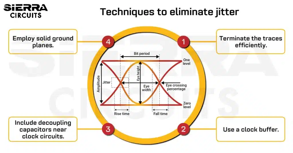
Benjamin: There has been a lot of work done by lots of folks on this. One of the best things you can do is start with the stack-up. Anytime you do a board design, even on a package design, the first thing you need to consider is what power domains you have and what your critical signals have, and then make sure you design stack-up to appropriately manage that. If you don’t do that, you are going to be forced into bad situations. If you are cost-constrained, you are going to have a stack up that performs poorly, having poor ground planes, or having too many ground plane cuts. That’s a big no. Ground plane cuts are very bad. Having not enough ground planes for all your return currents, the tight loops on the VRM side, these are all sorts of things you can do from an inductance perspective. And you can have some sort of transients if you do not have the right feedback capacity. These are the basics. There are plenty more, but stack-up is the fundamental thing.
How do you deal with low-speed PCB designs having high-speed switching problems?
Benjamin: It is all about managing your current. If your waveguides for your design are not appropriate, you have impedance mismatching or reflections in those channels, it is going to come out either as signal loss, EMI, or other problems with the channel.

High-Speed PCB Design Guide
8 Chapters - 115 Pages - 150 Minute ReadWhat's Inside:
- Explanations of signal integrity issues
- Understanding transmission lines and controlled impedance
- Selection process of high-speed PCB materials
- High-speed layout guidelines
Download Now
What are the best practices to design a highly reliable multilayer board for military applications?
Benjamin: There are some basics here. In the military world, we care about reliability. We typically operate just like automotive over a broader temperature range. One of the biggest things you see from a PCB design perspective is we do very dense HDI boards, high density interconnects. That means we have blind buried and through vias. There is a maximum lamination cycle. We are developing boards that go anywhere from 24 layers up to 40 plus layers that are mixed-signal with digital and RF. To make those boards work, we rely a lot more on blind and buried vias than through holes. We don’t care so much about the cost. And when you have all those vias, especially stacked on top of each other, there is a thermal expansion coefficient you have to consider. These designs and applications go through thermal expansions throughout their lifetime. It is going to be heated up and cooled down. Whether it is in space, or on an airplane, that doesn’t matter. As a result of this, there is a thermal expansion on the copper and you can have failures. A very common practice we do is staggering those via structures. That is a very common thing to do, but a lot of people can not afford the cost.

HDI PCB Design Guide
5 Chapters - 52 Pages - 60 Minute ReadWhat's Inside:
- Planning your stack-up and microvia structure
- Choosing the right materials
- Signal integrity and controlled impedance in HDI
- Manufacturing considerations for higher yields
Download Now
How much difference can occur between designed and manufactured controlled impedance specifications and how much is too much?
Benjamin: There are critical designs where you can specify more differences. There are certain folks in the industry that are looking to get well within that 5% range, but 10% is kind of the accepted standard when it comes to the difference between designed and manufactured controlled impedances. It depends on what signals we are talking about, how fast we are going, whether we are talking about DDR4, PCI gen three, gen four, ethernet standard, 400 GB across how many data pairs.

What is the degree of the feasibility of using BGA packages with lower parasitic inductances?
Benjamin: This comes down to the CCA or PCBA assembly. If you can support the layout and the cost to integrate, from a design perspective, after routing, the fanout is the first problem. The next problem is manufacturability. For most board assemblers right now can do 0.8 mm pitch. You are getting down in the smaller 0.6 to 0.4 mm but not everybody has the technology to assemble those sorts of BGA pitch patterns and afford the cost. Typically, the first thing you should do, if you’re designing a part, is to make sure the fab house and the assembler that you are working with can support the technology that you want to design. These are the primary limitations.
How do you determine loop mutual inductance between two signals/ return loops in a transmission line and how much is too much?
Benjamin: If you have a transmission line, the impedance is based on the root of L over C which is √L/C. So there is always a parasitic capacitance within the transmission line. You can create an extraction model for that transmission line. From that, you can know if there is too much inductive or capacitive. You can run a TDR on that extractive model. If you don’t have an extraction and you have raw artwork, you can measure with a TDR. With a TDR you will get impedance and you start with the voltage and you convert that. Anything positive on the transmission line is inductance. Anything negative is capacitance. You can integrate across that inductance and then you know how much inductance or capacitance is present on that transmission line.
What are the specific considerations for designing electronics for material selection, thermal management, and power management?
Benjamin: It starts with reliability. The factors to consider are: has it been deployed into space before, or flown on an airplane, been something that we have used before, the risk, the lifetime, the application, a Leo application or geo ( These are very different pieces of orbit and have different radiation requirements), the failure allowance, class-b or class-a requirement. These are the typical, basic starting points.
How important is power integrity in modern electronic design and can you describe its considerations?
Benjamin: Power integrity is everything for today’s electronics. It determines the success or failure of all electronic products today. If you think about it, we are making a system and that system is a transmission line and the transmission line carries the power. If that transmission line is matched appropriately to the source, to the load, your power is going to be delivered appropriately. If it is not, you can have problems. There are lots of other definitions of power integrity, but in general it is all about the quality of noise seen by the circuits on the dot. If that noise is greater than a certain amount, you will face problems.