


Contents

On-demand webinar
How Good is My Shield? An Introduction to Transfer Impedance and Shielding Effectiveness
by Karen Burnham
Choosing the right RF PCB components and placing them appropriately helps you avoid critical issues such as insertion loss and EMI. These errors generally occur due to poor isolation and parasitic effects.
As an RF engineer, you need to select low-noise amplifiers (LNAs), position oscillators close to the clock input pin, and place matching networks near mixer ports to significantly improve the overall performance.
In this article, you’ll learn how to integrate active and passive parts in radio frequency boards and the layout guidelines to follow when placing these parts. You’ll also learn the common assembly defects seen in radio PCB manufacturing and how Sierra Circuits addresses them to deliver high-quality circuit boards.
Watch the full webinar here: Design considerations and simulation for RF components
Highlights:
- Excessive spacing and poor grounding in RF boards increase insertion loss and impedance discontinuities.
- Incorrect amplifier selection degrades noise figure, linearity, and output power.
- Oscillator placement and isolation are critical for frequency stability.
- Parasitics from vias, pads, and traces distort radio signals.
Why component placement is critical in RF PCBs
In radio frequency designs, traces behave as PCB transmission lines rather than simple conductors. Even small layout discontinuities, such as excessive spacing, split ground planes, or poor isolation, can cause reflections, coupling, and radiation.
Understanding these constraints early helps designers avoid board respins and late-stage debugging.
Consider these scenarios when you’re planning your layout:
- Excessive component spacing might increase insertion loss and impedance discontinuities along the RF signal path.
- Insufficient isolation between adjacent traces and components might result in electromagnetic interference.
- Discontinuous or split ground planes beneath high-speed circuits might create large loop areas and voltage spikes.
- Incorrect orientation of RF PCB components such as filters, baluns, and impedance-matching networks might detune the intended response.
- Inaccurate thermal design for high-power devices (e.g., power amplifiers) leads to localized hot spots.
These issues often originate during early placement and routing decisions.
RF & Microwave Design Guide
8 Chapters - 44 Pages - 60 Minute ReadWhat's Inside:
- Basics of RF and microwave board design
- Choosing RF materials
- Trace, grounding, via, and stack-up design
- Component selection and placement
- Testing and isolation requirements to avoid interference
Download Now
How to integrate active components in radio frequency boards
When planning your radio frequency layout, you must ensure the amplifier meets noise and linearity targets, the oscillator remains frequency-stable, and the mixer provides clean frequency conversion.
Each device is highly sensitive to coupling, making proper selection and placement essential for reliable RF performance.
Let’s get into the details:
1. Pick an amplifier with a low noise figure (1-3 dB)
The choice depends on the application’s signal strength, frequency range, and linearity requirements. Consider the following factors to ensure the RF amplifier meets the system performance requirements:
-
- Gain
- Max input level
- Required linearity
- Operating frequency range
- Output power

Accurate impedance matching at both the input and output ports (typically 50 Ω) is essential to maximize power transfer and minimize reflections.
Also see the pros and cons of composite amplifiers for PCB designers.
3 parameters to consider when selecting the right RF amplifier
| Parameter | What it means | Significance | Selection and layout guidelines |
|---|---|---|---|
| Noise figure (NF) | How much noise the amplifier adds | Lower NF improves receiver sensitivity |
|
| 1-dB compression point (P1dB) | Output power where the gain drops by 1 dB | Defines the amplifier’s usable output power range |
|
| Third-order intercept point (IP3) | Linearity measure | Higher IP3 indicates better linearity and reduced intermodulation distortion |
|
Here are some examples of RF amplifiers.
| Manufacturer | Key specs |
|---|---|
| Analog Devices- ADL8141ACPZN |
|
| Analog Devices- HMC480ST89E |
|
| Mini-Circuits- PMA3-73-1W+ |
|
| MACOM- CMPA5585030F |
|

2. Ensure frequency stability with oscillators
Frequency stability can be achieved by maintaining solid ground, reducing noise coupling, ensuring clean power supply decoupling, and placing the oscillator close to the clock input. Poor placement can cause frequency drift, jitter, and unwanted emissions.
When selecting oscillators, you need to evaluate:
- Oscillator type (crystal, SAW, VCO)
- Sensitivity to nearby circuitry
- Phase noise

5 layout guidelines for oscillators:
- Position crystal oscillators as close as possible to the clock input pin to minimize signal degradation.
- Have a solid ground plane under the oscillator area. Follow your manufacturer’s reference layout for pad arrangement.
- Keep digital switching and high-current circuits away from oscillators.
- Isolate antenna feedlines from high-frequency oscillators to avoid coupling. For tips on antenna placement, see antenna integration and RF design guidelines for 5G PCBs.
- When using VCOs/PLL local oscillators, add decoupling capacitors with low ESR to provide a clean power supply.
Our design engineers worked on a board for a medical optical scanner. The main challenge was to manage the EM radiation from the inductor.
To address this, our experts optimized the placement of the oscillator and controller through an iterative layout process. The placement, as shown in the image above, ensures effective isolation from the inductor and switching regulator to minimize the risk of EMI. For more details, see case study: resolving EMI and PCB routing issues in a medical optical scanner.

Talk to a PCB expert: Book a meeting or call us at +1 (800) 763-7503.
3. Implement mixers for frequency conversion
Proper evaluation of mixer characteristics, combined with good isolation, impedance matching, and controlled signal routing, helps minimize conversion loss, distortion, and unwanted coupling.
Mixers are used for up-conversion and down-conversion in RF systems and are highly sensitive to layout and isolation.

4 design and layout guidelines for proper mixer performance:
- For RF mixers, you need to evaluate:
- Mixer type (active or passive)
- Conversion loss
- Port isolation (LO↔RF, RF↔IF)
- Intermodulation behavior
- Keep the LO trace short and route it away from sensitive RF and IF lines.
- Place baluns or matching networks as close as possible to the mixer ports to maintain impedance.
- Use via fences and ground stitching vias around the mixer section to suppress noise.
During the webinar, one of our attendees asked:
“When transitioning from stripline to microstrip and vice versa, ground vias are placed close to the transition. How important is it to stitch the ground planes together at other locations, and why?”
Ernie Frohring, Field Application Engineer, EMA Design Automation, replied:
“The importance of stitching ground planes together depends largely on the frequency of operation.
The farther away the stitching vias are from the transition, the less impact they have on the circuit’s performance. A useful way to think about this is in terms of wavelength. Ground vias are most effective when they are placed within approximately one-sixth of the wavelength of the operating frequency.
So, if you’re working in the gigahertz range, where the wavelength is about 6 inches per nanosecond, ground stitching within roughly 1 inch of the transition would have the most effect. Beyond that distance, the impact on signal integrity and return current continuity diminishes significantly.”
For more via design tips, see 4 RF PCB via design challenges with layout solutions.
7 strategies for integrating passive components in RF PCB layouts
- Choose a capacitor with an SRF higher than your operating frequency.

A capacitor’s impedance ideally decreases with increasing frequency. A capacitor’s impedance ideally decreases with increasing frequency. However, due to its inherent parasitic inductance, the impedance reaches a minimum at the self-resonant frequency (SRF), after which it begins to increase.
- Select components with a high Q factor. This results in lower insertion loss.
- For capacitors, choose NP0/C0G for stability where applicable.
- Use multiple parallel decoupling capacitors to cover a broad frequency range.
- Keep RF PCB components, such as inductors and baluns, close to the high-speed ports.
- Avoid routing between the component and its reference plane.
- Use RF chokes to filter out noise generated by switching power supplies.
To ensure RF designs perform as intended, simulation tools play a critical role. Cadence AWR tools offer a complete design workflow, from system simulation (VSS), RF front-end circuit design (AWR Microwave Office), to EM and antenna analysis (AXIEM, Analyst, Clarity 3D Solver). Further, their Celsius Thermal Solver tool analyzes reliability under temperature stress.
How to reduce parasitics in your high-speed boards
Parasitic effects can be minimized through reducing the trace length, optimizing via design, and the use of solid, low-impedance ground connections.
The most common layout-related parasitic issues and mitigation techniques are outlined below.
1. Parasitic inductance in pads, vias, and traces
Long or narrow current paths introduce unwanted inductance that degrades high-frequency performance.
How to reduce it:
- Place decoupling capacitors as close as possible to the power supply.
- Use short and wide traces.
- Position components with short connection lengths to minimize trace parasitic capacitance and inductance.
2. Via stubs creating resonances
Unused via stubs behave like resonant structures at RF frequencies, causing reflections and signal degradation.
How to reduce it:
- Incorporate blind or buried vias to eliminate stubs.
- Back-drill vias when blind/buried vias are not feasible.
3. Large ground return loops
Discontinuous or long ground paths increase loop inductance and radiated emissions.
How to reduce it:
- Keep ground paths short without splits.
- Place multiple stitching vias in a grid pattern to connect power and ground planes.

Ground stitching vias around an RF trace. - The spacing between two adjacent vias should range between λ/20 and λ/10, where λ is the signal’s operating wavelength.
In addition to the above considerations, PCB surface finish plays a critical role in maintaining signal integrity at millimeter-wave frequencies.
For designs operating above 20 GHz, surface finishes such as immersion silver, ENIG/ENEPIG, or hard gold are recommended. These finishes provide smoother copper surfaces and more consistent conductivity. This reduces conductor loss, impedance variation, and signal degradation in high-frequency applications.
How to select high-frequency connectors
High-frequency connectors are picked by matching their impedance, frequency range, mechanical fit, and electrical ratings.
Consider these guidelines:
- Make sure it fits into its footprint to prevent interfering with other components.
- Validate the connector’s I/O pins with your design requisites.
- Verify that the connectors support your design’s operating frequency range.
- Check the rated number of connector mating cycles for their reliable performance over the lifespan.
- Ensure connectors have adequate power and voltage ratings based on your design requirements to prevent overheating and voltage transients.
- Choose connectors with a characteristic impedance that matches your trace impedance (typically 50Ω,75Ω, 90Ω, and 100Ω).

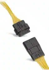
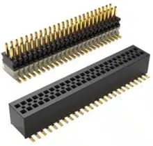
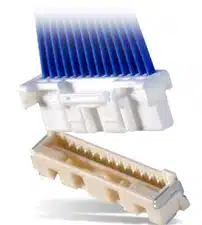
Wire-to-wire vs. board-to-board vs. wire-to-board connectors
Here you can have a quick look at the features of three types of connectors.
| Parameter | Wire-to-wire connectors | Board-to-board connectors | Wire-to-board connectors |
|---|---|---|---|
| Types | Butt connectors, splice connectors, multi-pin connectors | Mezzanine, stacking, and edge connectors | Pin headers, screw terminals, crimp terminals |
| Features |
|
|
|
| Applications | Automotive wiring, home appliances, and industrial equipment | Motherboard–daughterboard connections, stacked PCBs, modules | Power supplies, sensors, and peripheral devices |
| Examples | Molex Squba 1.80 sealed wire-to-wire connector
|
Samtec 0.80 mm board-to-board connector
|
Molex CLIK-Mate wire-to-board connector
|
For more, download the Connector Design Guide.
Connector Design Guide
5 Chapters - 32 Pages - 50 Minute ReadWhat's Inside:
- Basics
- Terminology
- Selection and layout rules
- Testing
- Application-specific PCB connectors
Download Now
3 tips to manage heat from RF PCB components
- Use a thermal pad beneath the power amplifier and connect it to an internal copper pour.

Copper pours in a PCB layout. - For higher cooling requirements, add a metal heatsink.
- Apply thermal interface materials (TIMs) between hotspots and heat sinks.

Thermal interface phase change material for heat dissipation in RF PCBs. - Ensure adequate airflow around heat sinks to enhance cooling efficiency.

Cooling fan and ventilation channels to dissipate heat in printed boards.
- Apply thermal interface materials (TIMs) between hotspots and heat sinks.
- Place an array of thermal vias under the device pad to transfer heat into the internal planes.
- For effective thermal conduction, design vias with a 0.3 mm (12 mil) diameter and a via-to-via spacing of 0.8 mm (31 mil) under power amplifiers.
For more heat dissipation techniques, see 12 PCB thermal management techniques to reduce heating.
2 common assembly defects observed by RF PCB manufacturers
1. Poor solder joints
RF components, such as baluns, filters, and metal shields, require precise soldering. Poor solder joints or excess solder might cause solder bridging and assembly errors.
Solutions offered at Sierra Circuits:
- We use a high-precision reflow oven with controlled temperature profiles to prevent component damage.
- We apply the correct amount of solder paste using a stencil to prevent bridging or cold joints.
- We run an X-ray inspection for fine-pitch components, such as QFNs and BGAs, to ensure accurate soldering.

Sierra Circuits fabricates high-quality RF and microwave boards with operating frequencies ranging from 10 MHz to 30 GHz. See RF and microwave PCB manufacturing services to learn more.
2. Pad voiding
A void is the hollow region inside a solder joint, typically caused by trapped flux gases, air pockets, or contaminants during reflow. These voids appear as dark spots during X-ray inspection and can impact both thermal and electrical performance.
Common issues:
- For thermal pads, voiding reduces heat dissipation efficiency.
- For signal pads, voids can increase resistance and degrade the signal integrity.
- Voiding in solder joints is evaluated based on the area percentage of the joint.
Solution offered at Sierra Circuits:
We follow IPC-A-610 and IPC-7095 guidelines to evaluate and ensure acceptable voiding levels in solder joints.
| Standard | Component type | Acceptable voiding |
|---|---|---|
| IPC-A-610 | General solder joints | ≤25% |
| IPC-A-610 | High-reliability joints | ≤5% |
| IPC-7095 | BGA/CSP solder balls | ≤25% |

The above X-ray inspection image from our shopfloor shows 14.08% voiding in the solder joint. This meets the IPC-7095 class 3 standard. The remaining 85.92% of the pad area is properly wetted and filled with solder.
Selecting the right RF PCB components and placing them appropriately helps prevent thermal issues, reduce signal loss, minimize parasitic effects, and improve EMI performance. Consider the guidelines provided in this article when you’re designing your next radio frequency board.
About the technical reviewer:
Dilip Kumar is the Senior Design Manager at Sierra Circuits with over a decade of experience in developing high-speed and HDI PCB designs featuring fine-pitch BGAs. He is proficient in Altium Designer, Cadence Allegro, Eagle PCB, KiCAD, and AutoCAD.
Leading a team of skilled PCB designers and layout engineers, he oversees projects from concept to production, ensuring precision and manufacturability at every stage. Dilip consistently delivers innovative, high-quality designs that meet demanding engineering and business objectives.
Need help designing an RF circuit board? Post your questions on our PCB forum, SierraConnect. Our design experts will resolve them.

About Pooja Mitra : Pooja Mitra is an electronics and communication engineer. With an experience of over three years in the PCB industry, she creates industry-focused articles that help electrical and PCB layout engineers.


Start the discussion at sierraconnect.protoexpress.com