


Contents
Weigh Design Choices for Solder Mask on Microwave PCBs
PTFE-based PCB laminates have long been the materials of choice for rf and microwave circuits because of their low loss tangents in those frequency domains. Though the processes to fabricate boards with PTFE-based laminates differ in several respects from those for conventional FR4-type materials, they are generally well-established at manufacturers and well-documented by the material suppliers with few exceptions. One aspect that may be unfamiliar to many PCB designers involves the treatment of copper post-etch and the implications for design to ensure good manufacturing yields.
Yield ultimately governs the cost of fabrication. If panels must be reprocessed because solder mask fails to adhere to blemished board traces, or worse—if panels must be scrapped—cost accrues.
Whatever laminate is used, PTFE or otherwise, the copper remaining after etch must be cleaned or automated optical inspection (AOI) to detect trace shorts or opens will be unreliable and solder mask will not stick. The best way to clean the copper is an abrasive scrub. However, all the suppliers of PTFE-based laminates advise that the laminate surface fresh from copper etching is best for adhesion and is compromised by scrubbing. There are alternative cleaning methods but none are as satisfactory as scrubbing to support AOI and solder mask adhesion.
Consequently, the copper is scrubbed before inspection. A plasma process is used after the scrubbing to reinvigorate the exposed laminate, to return the “tooth” to the surface so that solder mask will adhere, if it is an outside layer, or to aid subsequent lamination. However, the plasma oxidizes the copper, which must be cleaned again if solder mask will be applied. To avoid compromising the PTFE laminate surface by another scrubbing, a chemical clean for the copper follows in lieu of scrubbing, in preparation for solder mask. The panel must be dried immediately to eliminate moisture that could stain the copper and thereby inhibit solder mask adhesion. The process is a balancing act: Sometimes it doesn’t work and the solder mask has to be stripped, the panel has to be cleaned again and dried, and the solder mask reapplied.
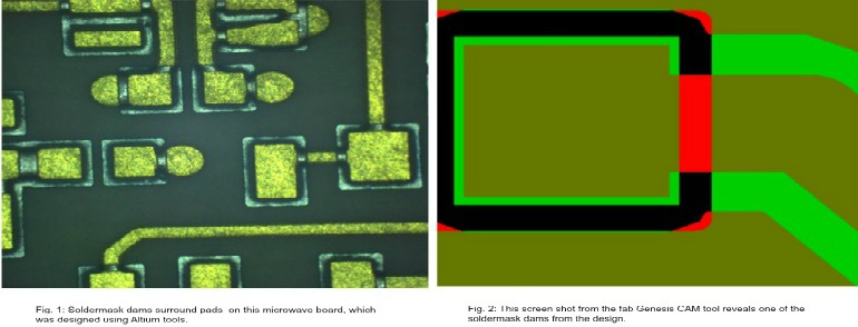
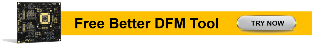
Instead of the standard practice of covering a board in solder mask, leaving openings for pads and so forth, rf and microwave designers commonly solder mask only the circuitry except for the pads, etcetera, leaving the PTFE laminate surface open. The copper can be scrubbed, AOI can be performed successfully, the soldermask is applied to the copper where it sticks, and there is no need to worry about it on the laminate because it develops off. Another common approach is to restrict the deposit of soldermask to little dams next to pads, which limit solder from traveling down the traces (Figure 1). This approach may be easy to implement for simple circuit, but tedious if thousands of dams are required (Figure 2).
The need for scrubbing or chemical cleaning of the copper can be avoided altogether, and therefore the need to plasma treat the surface of the PTFE dielectric if a lamination will follow, if gold is plated over the copper before etch. The gold does not oxidize, remaining bright after etch, so does not require cleaning to be ready for AOI.
Furthermore, a full solder mask with conventional solder openings can adhere to the board. Of course, gold is expensive but one or more cleaning processes and a plasma process are eliminated. There is with gold the issue of copper migration to consider. Over time, copper and gold tend to diffuse into each other, the copper brought to the surface oxidizes, and contact resistance increases as a result of the oxidation. Higher temperatures accelerate the process. Nickel ordinarily is used as a barrier layer between copper and gold to prevent diffusion, however nickel cannot be used for rf and microwave circuits.
At rf and microwave frequencies, the skin effect predominates in conductors: Most of the current flows in the outside of traces. Nickel is a lossy metal compared to copper especially at high frequencies, and the skin effect would tend to concentrate much of the current through the nickel near the trace surface. Copper diffusion into gold really is not a problem, unless the fabricated boards are kept in inventory a long time before assembly. Once components are soldered to their gold-plated contacts, there is no worry about contact deterioration.
Regarding the cost of gold, the plating amounts to a few microns thick. If there’s a plane on one side of the board, that would involve slightly more expense (more gold) than a signal layer, of course. Yet, there are fewer process steps with full-body plated gold. The copper is simply plated and then etched, with the gold as an etch resist, leaving the final metal surface finish.
Yield ultimately governs the cost of fabrication. If panels must be reprocessed because solder mask fails to adhere to blemished board traces, or worse if panels must be scrapped, cost accrues. For prototypes that are manufactured according to a flat price, that may make no difference to designers. But production quantities are a different story.
About the author: Atar Mittal is the Director and General Manager of design and assembly division at Sierra Circuits. He is responsible for the design and development of strategies and process automation tools for complex printed circuit boards and assemblies. Atar is also currently engaged in the development of productivity tools for electronics designers that would have a tremendous impact on shortening the development time.
About Atar Mittal : Atar Mittal is the General Manager and Director of the Design and Assembly Sierra Circuits division. He has a degree in Electrical Engineering from IIT Kharagpur and has worked in the electronics industry for over three decades.


