Contents

On-demand webinar
How Good is My Shield? An Introduction to Transfer Impedance and Shielding Effectiveness
by Karen Burnham
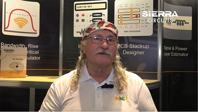
Daniel Beeker of NXP Semiconductors shared his insights about the techniques to avoid EMI in PCBs at PCB West 2022. Watch the full video to learn more.
What’s new in the field of EMC?
Daniel Beeker: One of the major challenges with simulation tools is the accuracy of their output. For instance, the results may say that your design is perfect but the system might fail. Further inspection of the PCB may reveal that there is a major discontinuity in the power supply that was missed by the simulation tool. As a designer, you need to be aware of these and should not completely rely on simulation tools.
Can you explain how switches create new spaces and moving EM fields?
Daniel Beeker: It’s a misconception that a switch connects a conductor and initiates the current flow in a loop. Generally, the energy is stored behind the switch, signal trace, and the EM field in the dielectric. The opposite side of the switch has a lower voltage and no electron displacement. When the switch is closed the EM field carries the energy and moves sequentially to the new connected space. It is like a water hose with a faucet. Initially, it seems like a short circuit with no output but after this short delay, the output can be observed (waves move at the speed of light).
How do trace spacing and layout influence EMC?
Daniel Beeker: From the perspective of radio emissions and robustness, proper trace spacing in the layout is extremely important. The trace should be one dielectric away from the ground plane. This creates a low-impedance transmission line to shield the signal from interference.
A signal propagating over a transmission line produces an EM field. If conductors are placed too closely, the energy of the aggressor trace will interfere with the victim trace. This impacts the magnetic and electric fields of the victim trace. Hence, understanding the nature of the signal and calculating the spacing between conductors is essential. It is preferable to route sensitive signals on the inner layers with ground pour on each side to isolate them.
PCB Transmission Line eBook
5 Chapters - 20 Pages - 25 Minute ReadWhat's Inside:
- What is a PCB transmission line
- Signal speed and propagation delay
- Critical length, controlled impedance and rise/fall time
- Analyzing a PCB transmission line
Download Now
Where should you place vias to avoid EMI?
Daniel Beeker: When the via is moving deep down the board stack-up, it is crucial to consider the dielectric layer change. For instance, a via on the outer layer connecting to the third layer through a ground plane (second layer) does not face any problem. If it has to connect the fourth or fifth layer, a ground transition via should be placed close to the signal via. It is a good practice to overlap the keep-out rings so that you can avoid routing between these vias.
How to handle ground planes for EMC?
Daniel Beeker: Implement a minimum etch approach to have maximum ground. Connect all the extra copper to the ground using vias. Delete the copper islands if you are unable to connect them to the ground. This will create a pseudo-Faraday cage on your circuit board. The increased copper surface area (top and bottom) will help distribute the ESD impulses across the board. This limits EMI as you have reduced the voltage applied to each square centimeter of the board surface.
In what circumstances would you use ground grids?
Daniel Beeker: Ground grids are used in large boards with a lot of layers. It is not recommended to implement it on outer layers as it creates copper wastage and pollutes the etching acid.
Is segregating sensitive components necessary for an EMC-friendly design?
Daniel Beeker: It is good to keep the aggressive signals away from sensitive components and their signals. For example, the disturbance in the analog to digital input should be kept minimal. Another sensitive circuit is an oscillator with a low voltage and amplitude. Its input is a Schmitt trigger which is easily disturbed by noise. When interfered, it will add extra counts in the PLL. Too many of these events can cause your system to reset.
Where would you place decoupling capacitors to reduce noise?
Daniel Beeker: Simple rule for capacitor placement is to use the 20th wavelength of the transistor switching speed. The capacitor must be kept as close as possible to the IC for a short travel time.
For a one nanosecond switching event, you can design a good power supply by placing the capacitor at half an inch of distance within the 20th wavelength. Typically for a BGA, the capacitor is situated between the pins on the bottom side of the board. For QFPs and similar packages, this is incorporated across the pair of leads.
Do you have signal termination strategies to help reduce EMI problems?
Daniel Beeker: For signal termination, you need to know the switching speed of the driver. If the distance between the driver and the receiver is more than a quarter of the wavelength, it will cause ringing. This adversely impacts signal integrity and EMC. To mitigate this, you should place a series resistor within the lump distance.
To learn how EMI and routing problems were successfully addressed in a medical device project, read our case study: resolving EMI and PCB routing issues in a medical optical scanner.
Daniel Beeker is the Technical Director at NXP Semiconductors with more than 45 years of experience in the electronic systems industry. He specializes in the development of microcontroller and microprocessor tools. Daniel also assists PCB designers worldwide with the layout techniques for EMC and signal integrity.
Note these things down for your next design since this comes from an industry expert. Please comment below if you require any assistance in building your board layout for signal integrity and EMC. Our design experts will be happy to help you.
Signal Integrity eBook
6 Chapters - 53 Pages - 60 Minute ReadWhat's Inside:
- Impedance discontinuities
- Crosstalk
- Reflections, ringing, overshoot and undershoot
- Via stubs
Download Now
About Sushmitha V : Sushmitha V has a master's degree in power electronics and has over four years of experience in the PCB industry. Her areas of interest include circuit board manufacturing, assembly, IPC standards, and DFM/DFA practices.


