


Contents
Designing a high-speed schematic in KiCad is simple due to its custom libraries and hierarchical design features. In this KiCad tutorial, you’ll learn how to create a high-speed schematic.
Designing a high-speed schematic in KiCad
The most important aspect of designing a high-speed schematic in KiCad is configuring grids, setting up design rules, and selecting appropriate components to handle high-frequency signals.
Step 1: Set up a new project
Launch the KiCad software and navigate to the main window. In the toolbar, click New Project. A dialog will open where you can name your project and select a directory to save it.

This will generate two key files: the schematic file (.kicad_sch) and the PCB layout file (.kicad_pcb).

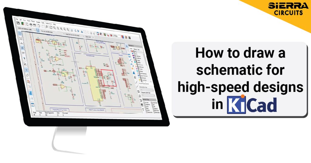
Step 2: Open the schematic editor
In the KiCad project window, click on Schematic Editor. The schematic editor window has a toolbar on the left for adding components, wires, and labels, while the top toolbar provides save, zoom, and design rules check (DRC) options.
The main window is your canvas, where you’ll place components and build your circuit.

The upcoming KiCad version 9 will introduce a new selection filter to the schematic and symbol editor, offering precise control over the elements selected during the editing process.
For step-by-step guidelines on designing a PCB using KiCad, download our eBook.

KiCad Design Guide
10 Chapters - 161 Pages - 180 Minute ReadWhat's Inside:
- Creating a component symbol library
- Setting up board parameters and rules
- How to route differential pairs
- How to place of components
Download Now
Step 3: Configure grid settings
The grid settings determine the precision with which you can place components and route traces. For high-speed designs, use a fine grid, typically 10 mil to 50 mil, to precisely align the traces.

This precision is necessary to ensure consistent trace lengths for differential pairs and minimize crosstalk.
Step 4: Set electrical rules in schematic setup
To define electrical rules, go to File and click on Schematic Setup.

Calculate the trace width based on impedance requirements to maintain good signal integrity. Generally, it is 50 Ω for single-ended and 100 Ω for differential pairs. Additionally, clearances between traces and other copper features should be set to minimize crosstalk and ensure adequate isolation.
Under Net Classes, you can define the wire and bus thicknesses, ensuring that high-speed signals are routed as desired.


Step 5: Select components for high-speed designs
Choosing the right components is crucial for high-speed circuit designs. Not all components can handle the demands of high-frequency signals, so selecting parts with appropriate specifications is essential.
For instance, when selecting capacitors for decoupling, it’s important to use low-ESR (equivalent series resistance) capacitors with high self-resonant frequencies, as these components are more effective at filtering high-frequency noise.
The choice of ICs, connectors, and passive components should be based on their ability to operate reliably at the intended signal frequencies.
FPGAs, microcontrollers, and memory devices must be chosen based on their maximum operating frequency, signal rise time, and input/output impedance. Consider the packaging of these components; smaller packages like QFN or BGA can reduce inductance and capacitance in the signal path, improving overall performance.
Step 6: Place the components efficiently
The schematic in KiCad is built by adding electronic components, such as resistors, capacitors, and ICs, from the symbol libraries. Go to Place, click Add Symbol, or press A (shortcut key). This opens a dialog where you can search for the component symbol you need.


KiCad includes a vast library of component symbols, but you can also import custom libraries if needed. Search for components by name or category and place them on the schematic by clicking. To rotate the component, press R.
To learn how to create custom libraries in KiCad, see creating schematic and symbol libraries in KiCad.
Place the components in high-speed data paths near their associated ICs to minimize trace lengths and potential signal degradation.
Implement termination resistors at the end of signal lines to match the trace impedance and absorb any reflected signals. This prevents signal reflections.
For more component placement tips, see component placement guidelines for PCB design and assembly.
Step 7: Connect components and route differential pairs
To connect components, click Add Wire in the right toolbar or press W key. Select a pin to start a wire and drag it to the destination pin to complete the connection.

Due to their high immunity to noise, differential pairs are ideal for sensitive signals like USB, HDMI, or high-speed clock lines.
In KiCad, differential pairs are defined by assigning them as pairs in the schematic and then routed using the differential pair routing tool in Pcbnew. When routing these pairs, it’s crucial to keep the two traces close together and ensure they have matched lengths. KiCad’s differential pair tool helps maintain consistent spacing and length matching, essential for preserving signal integrity.
Length matching is particularly important for differential pairs because any difference in trace length can result in skew, where one signal arrives slightly later than the other, causing timing issues.
Additionally, differential pairs should be routed with a consistent impedance, typically 100 ohms, to prevent reflections and maintain signal quality.
To learn the steps to route differential pairs in KiCad, see how to route differential pairs in KiCad.
Need help creating a high-speed schematic in KiCad? Our engineering team can assist you with schematic generation, symbol library setup, and impedance control for high-speed applications.
You can book a meeting with our experts or call us at +1 (800) 763-7503.

Step 8: Create a robust power distribution network
To add a power source, click Add Power and search for power symbols like VCC or GND in the component library. These symbols ensure that all components requiring power are connected to the same net.
Once placed, connect the power and ground symbols to the appropriate component pins using wires.

Place the decoupling capacitors as close as possible to the power pins of ICs to reduce the inductive effects. A combination of capacitors with different values filters out a broad range of noise frequencies. For example, in the image below, 10 nF capacitor filters high-frequency noise.

Bypass capacitors are similarly important for providing a local charge reservoir near high-speed ICs, helping maintain a stable voltage during sudden changes in current demand.
To receive an instant cost estimate for your PCB design with the KiCad UI, install the KiCad Quote Plugin.
Step 9: Annotate the schematic
After placing all the components and making the necessary connections, annotate your schematic to assign reference designators to each component.

Click Annotate Schematic in the top toolbar. This will automatically assign reference designators like R1, C1, U1, etc., to all components. You can manually adjust the annotations if needed.
Download our eBook for step-by-step guidance on creating custom libraries and linking symbols to footprints in KiCad 9.

KiCad 9 Step-by-Step Guide
6 Chapters - 41 Pages - 30 Minute ReadWhat's Inside:
- A complete KiCad 9 workflow from project creation to production file generation
- Step-by-step guidance on creating custom libraries and linking symbols to footprints
- Practical design checks: ERC and DRC
- Best practices for generating a clean BOM and fabrication-ready Gerber files
Download Now
Step 10: Run electrical rule check
Before proceeding to the PCB layout stage, check the schematic for electrical errors. Click Electrical Rule Check in the top toolbar. KiCad will analyze the schematic and report issues like unconnected pins or incorrect power connections.

Here’s an example of an ERC report.

You can configure the violation severity for the electrical rule check in the Schematic Setup.

Review the errors and correct them by making the required changes. Run a second ERC to ensure all the layout issues are resolved.
You can export the PCB BOM and netlist after finalizing the schematic. To directly transfer the schematic into the PCB layout, click Update PCB from Schematic.

Designing high-speed schematics in KiCad is efficient as it offers powerful tools like custom libraries, grid configuration, and differential pair routing. By carefully following best practices in schematic design, component selection, and electrical rule setup, you can avoid signal integrity issues in your PCBs.
Have queries regarding PCB design, manufacturing, and assembly? Post them on our forum, SierraConnect. Our experts will answer your questions.

About Sushmitha V : Sushmitha V has a master's degree in power electronics and has over four years of experience in the PCB industry. Her areas of interest include circuit board manufacturing, assembly, IPC standards, and DFM/DFA practices.


Start the discussion at sierraconnect.protoexpress.com