


Contents

On-demand webinar
How Good is My Shield? An Introduction to Transfer Impedance and Shielding Effectiveness
by Karen Burnham
Rick Hartley specializes in preventing and solving EMI and signal integrity problems. He is the principal engineer at RHartley Enterprises and has more than 50 years of experience in handling signal integrity issues.
Rick Hartley has been assisting designers in tackling challenges related to improving and maintaining good signal quality in PCBs for decades. Based on our interactions at PCB West 2018 and 2022, we created this article which gives his insights about design considerations to minimize EMI.
Here’s what Rick Hartley had to say.
1. Consider DFM guidelines when you design controlled impedance traces
“Controlling the impedance of the critical traces is essential for good signal integrity,” Rick said.
He added, “Designers today understand why controlled impedance really matters. They know the importance of terminating transmission lines and building a good PCB stack-up. What they are missing is the DFM, which impacts the fabrication process of their design. Understand the capabilities of the fabricator and build your design around it. Know what dielectrics and copper weights are available. Modify your trace width and circuit design accordingly to achieve the targeted impedance. This methodology will give you a better throughput from your board production.”

Features:
- Implements 2D numerical solution of Maxwell’s equation
- Supports 82 impedance models with multiple geometries such as coated, uncoated, and embedded microstrips and striplines
- Determines coupling coefficients for even and odd mode parameters
- Accounts for the trapezoidal shape of the trace
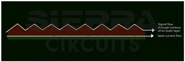
2. Energy-carrying fields are the primary reason for noise and EMI
At PCB West 2022, Rick Hartley said, “The real cause of signal integrity issues is not the voltage or current in the trace, but the field that carries energy. For example, digital circuits can create a strong field that can interfere with other analog circuits on the same board. This is called noise. If the same field corrupts other systems in the vicinity, it is called EMI. You can contain this field only through the right design procedures. For instance, an improper stack-up with a ground plane placed two or three dielectrics away from the signal/power layer will cause signal degradation.”

Features:
- Offers a library of build-up templates including single and sequential lamination
- Automatically chooses the type of board construction (coil/core)
- Allows you to design any controlled impedance traces
- Provides 3 technology levels (level I/II/III)
3. What Rick Hartley recommends to minimize losses in high-speed designs and improve EMI susceptibility
“When it comes to lowering losses in high-speed designs, the first thing we do is select a low Dk material,” Rick said during PCB West 2018. He continued, “Considering signal loss and attenuation is crucial in high-speed designs, especially in the gigabyte domain. Nowadays manufactured ICs have in-built pre-emphasis and equalization that alters the waveform shape at the driver and receiver ends to reduce losses. If the operating frequency of your design is a few GHz, it is sufficient to incorporate these ICs. If you are dealing with even higher frequency in tens of gigabytes, you will have to choose high-speed materials like I-speed.”
High-Speed Material Design Guide
6 Chapters - 19 Pages - 30 Minute ReadWhat's Inside:
- Importance of choosing the right material for your high-speed design
- Parameters that affect material selection
- Effect of dielectric constituents on your circuit board
- Characteristics of high-speed materials
- Effect of resin content and glass weave structure on your PCB
Download Now
Rick explained, “The concept of four signal steps rather than one can help to reduce loss tangent concerns and skin effect loss. Here, the idea is to create four different transitions similar to pre-emphasis. This changes the amount of energy per unit time drawn from the power bus and fed into the transmission line. You also have one clock signal for every four bits which quadruples the data rate. Hence, the clock rates per given data rate will reduce and improves the EMI susceptibility. On the contrary, you will have a smaller noise margin per step and so you have to be more careful about reflections, impedance control, and termination sizes.”
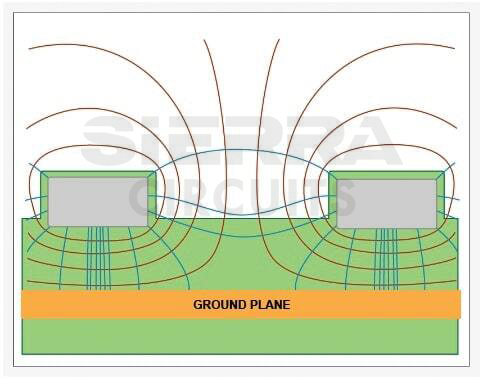
4. Place the reference plane close to the signal layer to avert EMI issues
“You already know, proper grounding provides a continuous return path for limiting the EMI. We attach systems to the Earth for safety and to avert high-energy fields like lightning. On the circuit board, even though it is not exactly ground, we add reference planes. The current in a trace creates electric and magnetic fields. To contain the fields and control the current, the line should be placed one dielectric away from the ground plane. If not, it will lead to grounding problems,” Rick advised.
5. Rick Hartley suggests fine-line routing for BGA
“With the trend of compact devices, the PCB industry is moving towards high-density interconnect.” Rick Hartley stated, “In some ways, the PCB industry has not kept pace with the miniaturizing ways of the IC industry. If you have a fine-pitch IC, you can branch the leads out off of the pattern. But with BGA, this is quite a problem because you will have to get lines out from a very tight pitch part. Breaking out a 0.5 mm BGA requires pretty fine line technology.” He believes fabricators can step up as there’s an absolute need for 1 and 2 mil technology.
6. High-performance PCB with a lower layer count is the way forward
“Taking the example of cost-driven IoT and automotive industries, where saving even one penny matters.”
He said, “Reducing the layer count is how they move toward it. They opt for a 3–4-layer high-performance PCB with good signal integrity. There are ways to achieve higher density and controlled impedance traces in lower layer count circuit boards. But, maintaining signal integrity is not an easy task.”
7. Choose quality over cost
“It is common to expect the best quality circuit boards at the lowest price, but this cannot be achieved without making compromises. You should never compromise quality for cutting costs. Circuits have failed and caused serious issues due to low-cost and cut-rate fabrication shops,” Rick said during the PCB2DAY workshop.
Incorporate these design recommendations in your next high-speed layout as it comes from Rick Hartley who is an industry expert. Please let us know in the comment section the signal integrity issues that you frequently come across in your designs. Our PCB design engineers will be happy to help you.

Signal Integrity eBook
6 Chapters - 53 Pages - 60 Minute ReadWhat's Inside:
- Impedance discontinuities
- Crosstalk
- Reflections, ringing, overshoot and undershoot
- Via stubs
Download Now
About Sushmitha V : Sushmitha V has a master's degree in power electronics and has over four years of experience in the PCB industry. Her areas of interest include circuit board manufacturing, assembly, IPC standards, and DFM/DFA practices.


