Contents

On-demand webinar
How Good is My Shield? An Introduction to Transfer Impedance and Shielding Effectiveness
by Karen Burnham
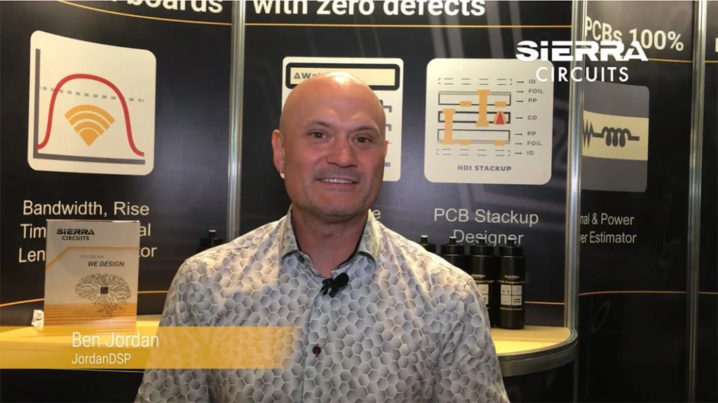
We ran into Ben Jordan of Jordan DSP LLC at the PCB West 2022 and had the privilege of discussing the best techniques for designing PCB antennas. Watch the complete video to learn more.
How do PCB antennas work?
Ben Jordan: It’s exactly like a high-speed digital trace that unintentionally behaves as an antenna. PCB antennas move charge in certain shapes which gives rise to propagation. They could be a stick of wire on a board surface or a dipole working with high-frequency alternate currents. In a high-speed circuit, the ground plane holds the charge so it doesn’t propagate. We do this to avoid noise and EMI problems. However, an antenna has to intentionally radiate and receive waves. Hence, they are deliberately kept away from the reference plane.
In what kind of electronics are antennas mostly used?
Ben Jordan: Everything’s wireless now. Antennas are incorporated from scanning information on a phone (near field communications) to sparse wide area networks using LoRaWAN. Hence, it’s necessary for PCB designers to learn about RF microwave antennas. You need to choose the right type and size of antenna that operates at the right frequencies. In addition, measure and match its impedance with a low-noise amplifier or a wireless microcontroller.
What are the key factors to design antennas for RF and microwaves?
Ben Jordan: First, determine frequency ranges like center frequency and bandwidth of operation. Also, understand the power level required. Next, size the antenna based on the layer stack. Set all the design constraints. These are all iterative processes. From the choice of material to the size of the antenna, it all plays a significant role.
PCB Material Design Guide
9 Chapters - 30 Pages - 40 Minute ReadWhat's Inside:
- Basic properties of the dielectric material to be considered
- Signal loss in PCB substrates
- Copper foil selection
- Key considerations for choosing PCB materials
Download Now
What are your best practices to design layer stacks for antenna boards?
Ben Jordan: The whole board stack-up doesn’t have to be of the same material. Usually, specialized materials are used on the surface layers. For example, you may have digital, RF, and analog signals in mixed-signal PCB. The key is to select the right material, but include it with cores and prepregs that are more general-purpose and stronger. Additionally, choose stack-up thicknesses suitable for RF and microwave PCBs and make manufacturing more economical. Once you have built a good layer stack, consult your fabricator for their insights.
Could you explain how to separate two patch antennas on a PCB?
Ben Jordan: Multiple patch antennas are used for more power and sensitivity. These are put into an array and those arrays are spaced at half or quarter wavelengths depending on the orientation. The direction should allow the far-field signals to increase signal strength or sensitivity.
What are your recommendations to mount PCB antennas?
Ben Jordan: There are two critical things for mounting antennas:
- Directionality: Typical IoT applications use fairly omnidirectional antennas. However, if they’re over a ground plane, then it will deplete the energy from the EM field of the antenna. Hence, it will disturb signal propagation. You can avoid this by using patches as the ground plane is a part of the transmission. Other types like inverted F and meandering antennas should be mounted away from the ground layer. But you should still connect them to a reference plane.
- Diversity: Mount antenna components at 90-degree angles to each other to improve reception over the entire sphere around the product.
What are the best materials for circuits with antennas?
Ben Jordan: The best materials are low-loss dielectrics, but it depends on the application. If it is for low-power and low-range ISM band applications like IoT, wifi, and Bluetooth, you can use regular FR4. When you are dealing with high power or longer range, you should consider loss and opt for Rogers dielectrics or other ceramic-filled materials.
Due to the lower Dk value, you need a bigger size object to match impedances. On the contrary, they have lower-loss tangents which are extremely important in patch arrays for increased power to travel long distances.
To learn how we routed antenna signals and differential pairs in a compact PCB layout, see our case study, designing microcontroller and functional PCBs with an antenna.
Are there specific tools that you recommend?
Ben Jordan: You definitely need a good simulation tool. ADS, Pathwave, Ansys, and HFSS, are flagship tools that model and simulate wave propagation of the microwave and RF designs. Subsequently, if you’re on a tight budget then you can use free tools like Qucs (open source). It has a harmonic balance and FTDD solver for electromagnetic simulation. As for designing the main printed circuit board, you have software packages like Altium, Eagle, and Auto Desk fusion 360. All these tools facilitate RF and microwave designing.
Ben Jordan is a computer system engineer from the University of Southern Queensland. He has 20 years of experience in the EDA industry. Before starting his own consulting and training company, he worked for Altium and Autodesk.
Hope you found this interview useful. Please comment below if you require any assistance in designing antennas for your PCBs.
RF & Microwave Design Guide
8 Chapters - 44 Pages - 60 Minute ReadWhat's Inside:
- Basics of RF and microwave board design
- Choosing RF materials
- Trace, grounding, via, and stack-up design
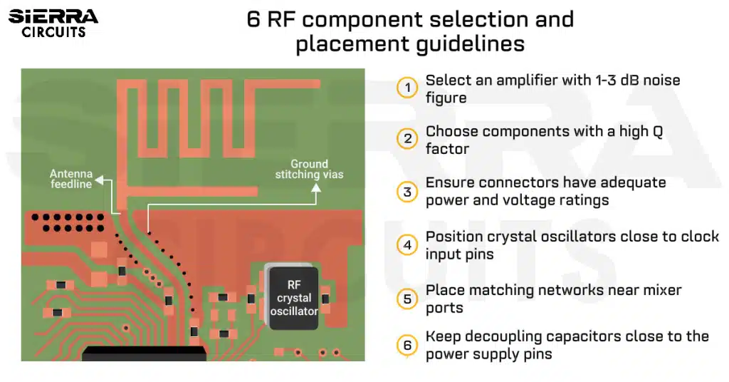
- Component selection and placement
- Testing and isolation requirements to avoid interference
Download Now
About Sushmitha V : Sushmitha V has a master's degree in power electronics and has over four years of experience in the PCB industry. Her areas of interest include circuit board manufacturing, assembly, IPC standards, and DFM/DFA practices.


