


Contents

On-demand webinar
How Good is My Shield? An Introduction to Transfer Impedance and Shielding Effectiveness
by Karen Burnham
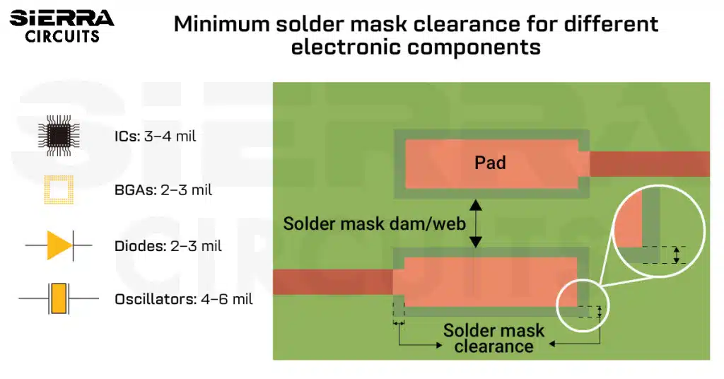
PCB solder mask clearance is the space between a copper pad and the surrounding solder resist. It typically ranges from 2 to 7 mil depending on the component.
Different parts, such as resistors, BGAs, and ICs, have distinct clearance requirements to ensure efficient soldering. For instance, BGAs need about 3 mil of clearance per side, whereas surface-mount resistors require around 2 to 3 mil.
As a circuit board designer, understanding these component-specific rules helps you prevent manufacturing defects like solder bridging, mask peeling, and misregistration.
In this article, you’ll learn the importance of solder mask clearance and the recommended values for different components.
Highlights:
- Too much mask clearance exposes traces, and insufficient spacing causes solder bridging or poor wetting.
- If the mask web between pads is below the manufacturer’s capability, implement gang masks to avoid potential soldering defects.
- Specify your mask clearances, pad definitions, via treatments, and minimum dam widths in the fabrication notes.
Why is solder mask clearance important in PCB design?
The solder mask opening (clearance/expansion) determines how accurately pads on circuit boards are exposed for soldering. It is a key DFM parameter that directly affects solder joint quality and the overall board reliability. Solder mask openings are implemented during the layout phase for the solderability of components.
Component footprint (pad size) is considered for calculating solder mask clearances.
- The component footprint defines the solder mask clearance for design and manufacturing.
- Pad size and spacing determine the values of mask expansion and web.
Accurate mask openings ensure pads are properly exposed for perfect soldering.

Clearance values are not arbitrary; they must strike a balance between manufacturing capability and electrical safety.
The ideal clearance depends on your PCB manufacturer’s registration accuracy and the minimum mask web or dam (the smallest strip of solder mask that can be reliably placed between pads).
Too much solder mask clearance can expose nearby copper traces, increasing the risk of shorts. On the other hand, too little clearance can cause the resist to overlap the pad edges, which may trap solder and lead to solder mask errors.

If the mask web between pads is below the manufacturer’s minimum capability (typically 4 to 7 mil), implement gang masks where all openings are merged, as shown below.

Download the Design for Manufacturing Handbook to learn more about prototyping.

Design for Manufacturing Handbook
11 Chapters - 96 Pages - 90 Minute ReadWhat's Inside:
- Annular rings: avoid drill breakouts
- Vias: optimize your design
- Trace width and space: follow the best practices
- Solder mask and silkscreen: get the must-knows
Download Now
Solder mask expansion rules for different electronic components
The ideal solder resist clearance depends on the pad size, component pitch, and your fabricator’s registration tolerance.
Here are recommended solder mask clearances for design and manufacturing:
1. ICs, resistors, and capacitors
Solder mask clearance for standard ICs and passive components typically ranges from 2–6 mil per side, depending on the component pitch and body size.
| Pitch | Recommended mask expansion (per side) | Minimum solder mask web |
|---|---|---|
| Fine-pitch (<0.65 mm) | 2–3 mil | ≥3–4 mil |
| Standard pitch (0.65–1.27 mm) | 3–4 mil | ≥4 mil |
| Large body (>10 mm) | 4–6 mil | ≥5 mil |
For very fine pitch (<0.5 mm), confirm that the fabricator can maintain solder mask dams ≥3 mil; otherwise, use gang openings.
Read our knowledge base on PCB surface to learn more about different board layers.
2. Ball grid arrays
BGAs require tight solder resist opening, typically 1 to 4 mil per side, because even small mask-to-pad misalignment can affect ball landing and joint reliability.
| Ball pitch | Recommended mask clearance (per side) | Minimum solder mask dam |
|---|---|---|
| Fine-pitch (<0.5 mm) | 1-2 mil | ≥2–3 mil |
| Standard pitch (0.5–0.8 mm) | 2-3 mil | ≥3–4 mil |
| Coarse pitch (>0.8 mm) | 3-4 mil | ≥4 mil |
For micro-BGAs (<0.4 mm pitch), SMD pads may be required due to limited space; coordinate this with your assembler early in the design phase.
Stick to these guidelines when designing solder mask expansion for BGAs:
- Use NSMD pads for improved solder joint reliability.
- Make sure the copper pads are approximately 80% of the ball size to ensure proper solder volume and joint formation.
For more details, see solder mask-defined pads vs. non-solder mask-defined pads.
3. Inductors, diodes, and other discrete devices
These electronic components come in various sizes and require different solder volumes. So, when you design mask openings, match them to the part’s size and solder needs. Discrete components generally need 2 to 8 mil of solder mask clearance per side. Larger packages require additional relief to tackle mechanical and thermal stress.
| Package type | Recommended mask expansion (per side) | Minimum solder mask web |
|---|---|---|
| Small (SOT-23, LEDs 0603) | 2- 3 mil | ≥3–4 mil |
| Medium (SOT-89) | 3-4 mil | ≥4 mil |
| Large/through-hole (TO-220) | 4-8 mil + relief | ≥5 mil |
For high-current devices, ensure the solder resist dams meet the fabricator’s required minimum width (typically >4 mil for green mask) to prevent solder bridging during wave soldering.

4. Connectors, crystals, and oscillators
These components are mechanically stressed during insertion or operation and usually require 3 to 8 mil of solder mask expansion per side to prevent mask cracking and ensure stable mechanical anchoring.
| Pitch | Recommended mask expansion (per side) | Minimum solder mask dam |
|---|---|---|
| Fine-pitch (<1.0 mm) | 3-4 mil | ≥4 mil |
| Standard pitch (1.0–2.54 mm) | 4-6 mil | ≥5 mil |
| Large body (>10 mm) | 6-8 mil | ≥6 mil |
When defining solder mask openings for crystals, connectors, and oscillators, add extra resist clearance around mounting holes to prevent cracking. Keep the anchor pad openings slightly oversized to avoid mask chipping. These small adjustments significantly improve manufacturability and reliability.
5. Relays and switches
Relays and switches need oversized solder mask openings to tolerate mechanical and thermal stress during operation and soldering. They require 4 to 6 mil solder resist relief around through-hole leads.
For better results:
- Expand solder resist openings slightly larger than pads to accommodate alignment errors and mechanical stress.
- Add extra clearance around mounting holes and anchor pads to prevent solder mask cracking.
- Use SMD pads on anchor tabs in high-vibration environments for stronger mechanical anchorage.
For relays with large current loads, ensure the solder resist does not overlap copper pours to avoid localized delamination.
6. Through-hole components
Through-hole components need 4 to 6 mil (0.1 to 0.15 mm) solder mask clearance to keep the mask out of the barrel.
For wave soldering, mask clearance should be slightly increased, up to 8 mil (0.2 mm), to account for solder wave turbulence.
Solder resist clearance for test points
Test points require precise solder mask openings to guarantee consistent probe contact and prevent accidental solder bridging. Maintain 3–5 mil (0.075 to 0.13 mm) solder resist clearance around test pads.
Follow these DFT practices when designing test points:
- Design test points with 30 to 50 mil (0.76 to 1.27 mm) pad diameters to ensure proper contact between the probe tips and pad.
- Leave some test points unmasked for easier electrical access.
- Group test points consistently and use uniform solder resist clearance.
- Unmasked test points should be located away from high-density fine-pitch areas to prevent accidental solder bridging.
Sierra Circuits fabricates and assembles PCBs with minimum solder mask dams of 4 mil. Check out our PCB manufacturing capabilities to learn more.
8 best practices for solder mask design in PCBs
When defining solder mask openings, the goal is to achieve reliable solder joints while preventing defects like bridging or exposed copper. These general guidelines help ensure manufacturable and consistent results across different board technologies.
- Use NSMD pads with positive mask expansion for most SMT components. This is the standard practice as it provides better registration tolerance and stronger solder joints.

Non-solder mask defined pad with a fully exposed copper land pattern on a PCB. - Avoid 1:1 mask-to-copper openings unless you’re using SMD pads for a specific purpose, such as large thermal pads or fine-pitch BGAs where the solder resist defines the solderable area.
- Keep copper features at least 4 to 6 mil away from the edge of a solder resist opening to protect against registration shift.
- Maintain minimum solder mask dam widths of ≥4 mil for green, 5 mil for blue, 5 mil for red, 6 mil for black, and 7 mil for white.
- Reduce expansion or implement a gang mask if the dam requirements are less than the manufacturer’s capability.

Gang solder mask opening. - Opt for via tenting when the finished hole size is ≤12 to 14 mil (0.30 to 0.35 mm). Smaller tented vias (<10 mil or 0.25 mm) are more reliable, as the mask can fully cover the via without voids.
")
IPC-4761 type I(b) tented vias are covered with a solder mask layer on both sides. For more design for manufacturing rules, see solder mask layer in PCBs: top 4 DFM guidelines.
-
Follow the IPC-4761 standard for via filling, plugging, or capping critical holes such as via-in-pad.

IPC-4761 type VII via filling. - Verify your manufacturer’s capabilities for mask registration, minimum web/dam, and any color-dependent limits before finalizing your design.
Things to include in your fab notes on solder mask
When defining solder mask requirements in your fabrication notes, make sure to include the following details to ensure manufacturability and reliability:
- Solder mask registration tolerance: Specify a registration tolerance of ±2 mil (0.05 mm) or better to ensure accurate alignment between mask openings and copper features.
- Mask-to-pad clearance: The solder mask should not overlap copper pads unless SMD pads are explicitly required. Allow CAM operators to fine-tune mask apertures to maintain the minimum web and registration tolerances, but do not permit encroachment on component pads.
- Mask expansion for SMT pads: Unless otherwise noted, define a solder mask expansion of 4 mil (0.1 mm) per side for all surface-mount (SMT) pads.
- Minimum mask web (or dam): Maintain at least 4 mil (0.1 mm) of solder mask between adjacent pads. If this spacing isn’t achievable, specify to merge openings (gang mask) as per DFM guidelines.
- Pad type: Use NSMD pads for standard components. Use SMD pads only for fine-pitch BGAs (<0.4 mm pitch) or thermal pads where required.
- Via tenting and filling requirements:
- Tented vias: All vias ≤12 mil (0.30 mm) diameter should be tented on both sides.
- Filled vias: Vias should be filled and capped according to IPC-4761 Type VII standards.
- Solder mask type and color: Specify liquid photoimageable (LPI) solder mask, green preferred unless otherwise noted. If you’re using another color, verify its minimum web capability with your fabricator.
Download the PCB Fab and Assembly Notes for Designers.

PCB Fab and Assembly Notes for Designers
8 Chapters - 72 Pages - 70 Minute ReadWhat's Inside:
- Guidance on how to write comprehensive fab documentation
- Advanced fabrication notes for flex, rigid-flex, and hybrid stack-ups
- Difference between fabrication and assembly notes
- Assembly documentation essentials: BOM, X-Y data, and drawings
Download Now
Following the right solder resist clearance rules based on your components helps you avoid shorts and ensure reliable solder joints. Always check your PCB manufacturer’s capabilities before finalizing values.
About the technical reviewer:
Dilip Kumar is the Senior Design Manager at Sierra Circuits with over a decade of experience in developing high-speed and HDI PCB designs featuring fine-pitch BGAs. He is proficient in Altium Designer, Cadence Allegro, Eagle PCB, KiCAD, and AutoCAD.
Leading a team of skilled PCB designers and layout engineers, he oversees projects from concept to production, ensuring precision and manufacturability at every stage. Dilip consistently delivers innovative, high-quality designs that meet demanding engineering and business objectives.
Have queries regarding solder mask clearances? Post them on our community, SierraConnect. Our design experts will answer them.

About Mohamed Faheemuddin : Mohamed Faheemuddin is a mechanical engineer. His passion for electronics drew him to the PCB industry. With an experience of over 3 years in the PCB industry, he specializes in developing articles for engineers and hardware designers.


Start the discussion at sierraconnect.protoexpress.com