


Contents

On-demand webinar
How Good is My Shield? An Introduction to Transfer Impedance and Shielding Effectiveness
by Karen Burnham
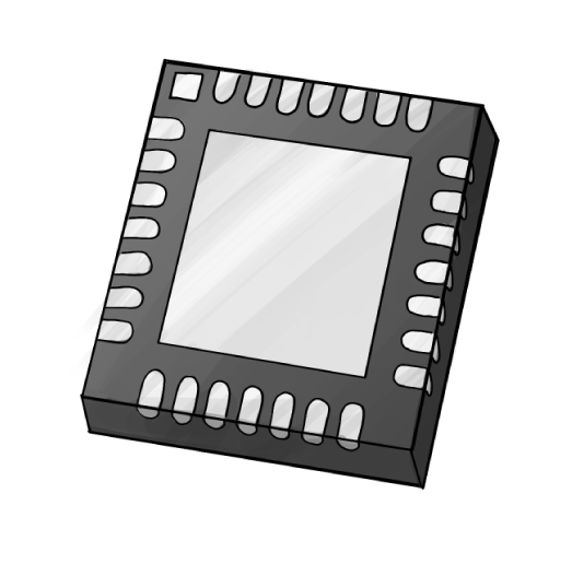
Quad flat no-lead packages are leadless surface-mount ICs. They offer a small form factor and efficient thermal performance. These miniature devices are suitable for consumer electronics, automotive designs, and industrial applications.
Highlights:
- Choose QFN variants (TQFN, VQFN, MLF) based on height, thermal, and application needs.
- Use side wettable flank pads for reliable solder joints and easy AOI inspection.
- Follow manufacturer datasheets for footprint, thermal pad vias, and paste mask design.
- Prefer QFN over QFP for a better thermal performance.
In this article, you’ll learn about QFN, its construction, and key footprint design best practices.
What does QFN stand for?
QFN, short for quad flat no-lead, is a leadless package type that electrically connects the silicon die directly to the PCB pads through its bottom terminals and a central exposed pad.
What’s inside a QFN package?

A quad flat no-lead package has a silicon die mounted on an exposed copper-alloy lead frame using epoxy, connected through wire bonding or flip-chip technology, with terminal pads along the bottom edges and a central exposed thermal pad for grounding and heat transfer.
The QFN packages come with a die surrounded by a lead frame. The lead frame is made up of a copper alloy with a matt tin coating.
The die and the frame are usually connected to each other using wire bonding. Copper/gold is usually preferred for wire bonding. Some manufacturers use flip-chip technology for this interconnection. The flip-chip technique offers better electrical performance compared to the conventional one.
The metalized terminal pads are located on the bottom surface. These terminal pads are present along the four edges of the bottom surface and provide electrical interconnections to the PCB.
The bottom side of the package consists of an exposed pad. This pad provides an efficient heat path to the PCB. The exposed pad enables ground connection as well.
The QFN package is soldered to the circuit board at the exposed pad. The die attach is the epoxy material used to fix the die to the exposed pad.
For heat dissipation methods, check out 12 PCB thermal management techniques to reduce PCB heating.
The following are some of the properties of standard QFN packages:
- 0.35mm to 2.10mm maximum seated height (standard: 0.85 mm)
- Terminal platings of Ni-Pd-Au and Sn
- Halogen-free and lead-free
- RoHS, ELV, and REACH compliance
The commonly used variants of QFN packages include thin QFN (TQFN), very-thin QFN (VQFN), micro lead-frame (MLF), etc.

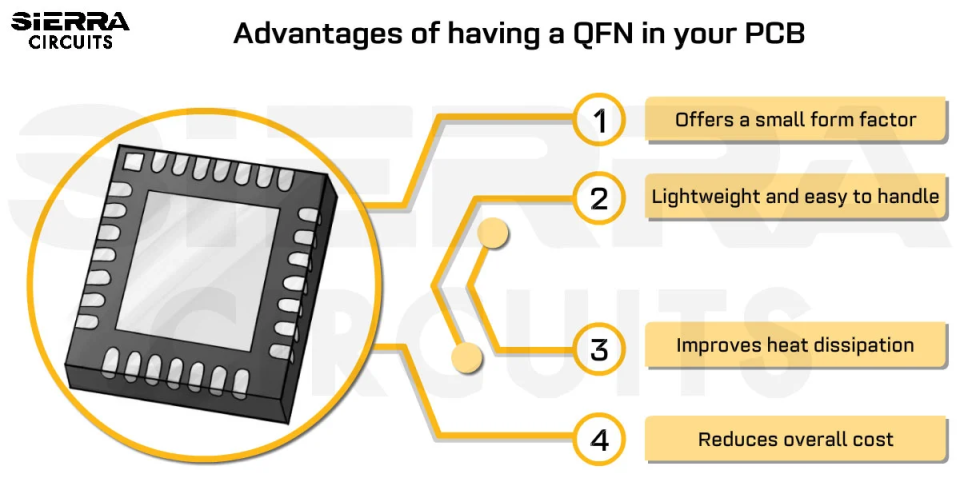
6 advantages of having QFNs in your PCBs
Here are the benefits of using QFN packages in your PCBs:
- Quad flat no-lead packages come in lightweight and are easy to handle.
- These packages are available in a thin profile and a small form factor.
- The bond wires used to connect the die and frame are short.
- The lead inductance of these packages is low.
- They are ideal for applications that require good heat dissipation.
- These packages are easily available at a low cost.
What are the different types of QFN packages?
Quad flat no-lead packages are classified into punch-type (single mold cavity) and sawn-type (mold array process) based on their molding and singulation methods.
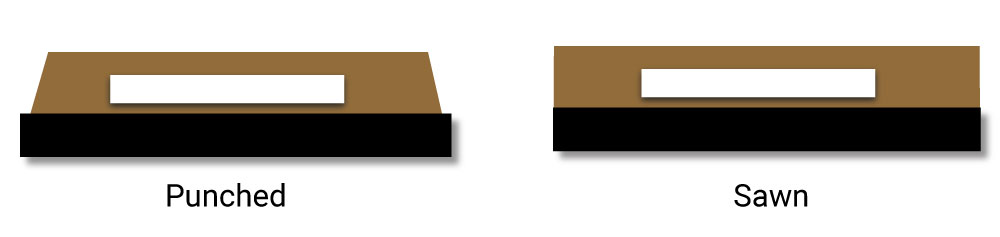
Punch-type
In punch-type singulation, the package is molded in the single mold cavity format and is separated using a punch tool. This means that only a single package is molded into shape using this method.
Sawn-type
These packages are molded using the mold array process (MAP). This method involves cutting a large set of packages into parts.
A final saw process helps to separate the sawn-type packages into individual packages.

HDI PCB Design Guide
5 Chapters - 52 Pages - 60 Minute ReadWhat's Inside:
- Planning your stack-up and microvia structure
- Choosing the right materials
- Signal integrity and controlled impedance in HDI
- Manufacturing considerations for higher yields
Download Now
What are the types of terminal pads used in QFNs?
QFN terminal pads are available in fully exposed, pull-back, and side wettable flank designs, each optimized to improve solder joint reliability and ease of inspection.
Fully exposed terminal ends

In this type, the terminal ends are fully exposed all the way to the edge of the package and to the side of the package.
Pull-back terminal ends

The terminal ends are pulled back from the edges of the package. Solder fillets are not added after the reflow soldering process for this type of terminal end package.
Side wettable flank terminal ends
These types of terminal ends are an altered form of fully exposed terminal ends. Side wettable flank terminal ends enable solder wetting for the formation of solder fillets. The solder failure inspection using AOI becomes easier if uniform solder fillets are formed. This eliminates the need for X-ray inspection.
How to design footprints for QFNs?
When designing a QFN footprint, always refer to the manufacturer’s datasheet for the package outline drawing. This ensures accurate pad dimensions, proper ground pad via placement, correct solder mask/paste openings, and clear orientation markings, critical for reliable assembly and optimal thermal performance.
The detailed package outline of an HVQFN48 package from NXP is given below:

The following things must be taken care of while designing the footprint of a QFN package:
- Orientation marking/pin 1 marking.
- The ground pad (EP pad) should have a sufficient number of vias for heat dissipation.
- Check the solder mask and solder paste layers. Keep the openings as recommended by the manufacturer.
- Solder web should be 4mil or more.
The figure below shows the recommended footprint for the same HVQFN48 package:

How are QFNs assembled?
QFNs are assembled using a surface-mount process that includes solder-paste printing, precise pick-and-place, pre-reflow inspection, reflow soldering, and post-reflow inspection to ensure reliable electrical connections and efficient heat transfer.
The following are the basic steps involved in the surface-mount assembly of the QFN components:
- Solder-paste printing: Solder paste printing is the process of uniformly spreading the solder paste on the board before the placement of components.
- Component placement: The QFN IC components are mounted on the circuit board as per the layout decided during the PCB design stage. Since these components have high interconnection density, precise and accurate pick and place tools are used.
- Pre-reflow inspection: Pre-reflow inspection is done to ensure that the board is ready to go into the reflow oven. This helps to remove contaminants on the surface of the board that may interfere with the soldering process.
- Reflow soldering: QFN components are commonly soldered using reflow soldering.
- Post-reflow inspection: This inspection is done to check the quality of the soldering.
A proper PCB footprint and stencil design are required for the assembled components to operate as per the design intent.
Also read, Thermal profile for solder reflow.
How are the QFN solder joints inspected?
Since QFN solder joints are hidden beneath the package, they are inspected using optical methods where possible and X-ray imaging to verify joint integrity and detect voids or defects.
Rework on assembled components
QFNs can be reworked using precision stations with alignment tools and hot-air heating for safe removal and replacement.
If a defect is noticed post-assembly on any QFN component, that particular component can be removed and replaced. Special rework stations are available for this purpose. A rework station should have the following components.
- Split-light system: acts as a vision system to observe the bottom side of the package and the site on the PCB.
- An X-Y table for alignment.
- A hot-air system with top and bottom heaters for component removal.
The procedure for rework is given below.
- A pre-bake process is done before heating to avoid any moisture-related failures of the board and the components.
- The next step is de-soldering, and the temperature profile of the board and the components should be kept in mind.
- Once de-soldering is done, the component should be mechanically removed. For large components, pipettes can be used, and for smaller ones, tweezers are a good option.
- After removal, the PCB pads should be cleaned to remove any solder residue. This also prepares the site for the new component placement.
- The placement of the new component takes place through the same steps mentioned earlier during assembly.
To pick the appropriate board type for microchips, see how to choose the right PCBs for IC integration.
What is the difference between QFN and QFP?

QFP packages feature gull-wing leads extending from all four sides, and QFN packages feature leadless bottom-pad connections.
| Feature | QFN | QFP |
|---|---|---|
| Leads | Leadless bottom-pad connections | Gull-wing (L-shaped) leads extending from all 4 sides |
| Assembly | Bottom-side soldering, precise placement required | Good footing from extended leads, easier handling |
| Pin Count | Varies by package size | 8-70 pins per side (QFP32, QFP64, etc.) |
| Pin Spacing | Matches pad pitch (typically 0.4-0.8mm) | 0.4mm to 1mm pitch |
| Variants | TQFN, VQFN, MLF | TQFP, VQFP, LQFP |
| Footprint | Exposed pad + perimeter pads | Leadframe with extended gull-wing leads |
| Inspection | X-ray required (hidden joints) | Optical inspection possible |

Design for Manufacturing Handbook
11 Chapters - 96 Pages - 90 Minute ReadWhat's Inside:
- Annular rings: avoid drill breakouts
- Vias: optimize your design
- Trace width and space: follow the best practices
- Solder mask and silkscreen: get the must-knows
Download Now
What is an LQFP64 package?
LQFP64 is a low-profile QFP variant with 64 pins, 1.4mm body thickness, and 2mm lead-frame footprint, offering similar advantages to standard QFP.
Because of their small size and heat-dissipating characteristics, QFN IC packages are widely used. The available QFN variants are suitable for a broad range of applications. Hence, QFN packages are in high demand when it comes to surface-mount packages.
Let us know if you have any queries about QFN on our forum, SierraConnect. Our experts will answer them.

About Milan Yogendrappa : Milan Y is an electronics and communication engineer with over 6 years of experience in developing and editing technical articles related to PCB design, manufacturing, and assembly. He is currently the editor-in-chief at Sierra Circuits.


Start the discussion at sierraconnect.protoexpress.com