Contents

On-demand webinar
How Good is My Shield? An Introduction to Transfer Impedance and Shielding Effectiveness
by Karen Burnham
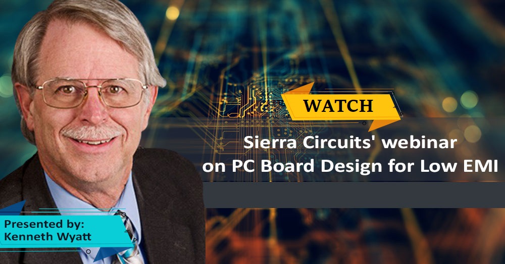
Watch this webinar on PCB design for low EMI presented by Ken Wyatt, Principal Consultant at Wyatt Technical Services LLC (Colorado).
WATCH WEBINAR
Abstract: PCB Design for Low EMI Webinar
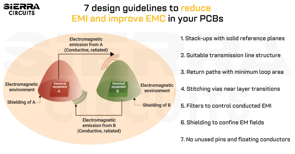
As a consultant for over 10 years, I’ve had a chance to perform design reviews or help troubleshoot hundreds of products. In so doing, I’ve realized the root cause of many design issues revolves around the circuit board design. Poor board designs can result in radiated emissions, radiated immunity, and electrostatic discharge (ESD) compliance failures, among others. Bad board designs often result in endless cycles of trial and error mitigation – compliance testing – board spins – and more troubleshooting/mitigation/spins. This drags out the schedule and is very costly.
I’ll explain why reducing circuit loop areas is only part of the solution and to understand proper board design for lowest EMI requires understanding how signals propagate in boards. Once you understand signals move via electromagnetic fields, then board stack-up and trace routing should become very clear and you should be able to design a low-EMI board the first time!

High-Speed PCB Design Guide
8 Chapters - 115 Pages - 150 Minute ReadWhat's Inside:
- Explanations of signal integrity issues
- Understanding transmission lines and controlled impedance
- Selection process of high-speed PCB materials
- High-speed layout guidelines
Download Now
Preview: PCB Design for Low EMI Webinar
As an EMC consultant for over 10 years, I’ve had a chance to review or help troubleshoot hundreds of electronic products. I find that most of those products that fail compliance testing are due to poorly designed PC boards. In this presentation, I’ll show you design techniques for reducing the EMI risk of your board.
There are only three things you can do with electromagnetic fields. They can either be stored, moved, or converted to kinetic energy. To propagate an electromagnetic wave requires a transmission line comprised of two pieces of metal, usually separated by a dielectric. In the case of a standard PC board, this would be the microstrip or stripline and a return plane.
This is the cross-section of a standard microstrip we’re all familiar with. You can see the H field flux wraps around the trace while the E field is mainly concentrated between the trace and return plane. As we’ll see in a moment, the actual signal in the form of an electromagnetic wave travels through the dielectric space between the trace and return plane. The trace merely serves as a way of guide and guides the path of the signal energy.
We’ll discuss the actual physics of way of propagation in PC boards shortly. But one important concept to understand is that for low-frequency signals, the return conduction current path is relatively spread out along the return plane and mostly takes a direct path from load back to the source. We call this the path of least resistance. So what constitutes low frequency? Something less than 50 to 100 kilohertz. So this concept is most important for audio or other low-frequency technologies.
For high-frequency signals, return conduction current path is relatively confined along the return plane and directly underneath the signal trace. We call this the path of least impedance and is due to mutual inductance between the trace and plane. So what constitutes high frequency? Well, something greater than 50 to 100 kilohertz. So this concept is most important for most other digital and RF technologies.
Here’s a simulation of this concept. With the return conduction current in green, for the 1-kilohertz example on the left, we see the return current is spread out and basically travels from the load directly back to the source. In the 1-megahertz example on the right, we see the return current located directly underneath the circuit trace. This will be very important when we partition our circuit board between analog and digital circuitry.
So let’s discuss just how signals move in circuit boards. This will likely be your most important takeaway during this presentation. Most of us designers have been misled in our circuits class. It was at least implied that the current was electrons flowing through copper wires from source to load. And for DC circuits and ignoring the initial turn-on transient, this is accurate. However, the movement of electrons does not occur at near light speed. They are too tightly bound to the copper molecules and only move at about one centimeter per second.
For AC circuits, the standard circuit theory model cannot be modeled as simple wires but as transmission lines. We’ll go into the actual physics of signal propagation in a moment. But understanding how digital signals propagate in PC boards will give you a competitive advantage over other companies who may not understand this to how signals move in PC boards, the circuit’s point of view and the field’s point of view. In reality, they are related. That is you can’t have one without the other. Now the circuit theory point of view considers only the signals and power return back to their source.
WATCH WEBINAR
Ken Wyatt Bio
Kenneth Wyatt is principal consultant of Wyatt Technical Services LLC and served three years as the senior technical editor for Interference Technology Magazine from 2016 through 2018. He has worked in the field of EMC engineering for over 30 years with a specialty is EMI troubleshooting and pre-compliance testing. He is a co-author of the popular EMC Pocket Guide and RFI Radio Frequency Interference Pocket Guide. He also co-authored the book with Patrick André, EMI Troubleshooting Cookbook for Product Designers, with forward by Henry Ott. He is widely published and authors The EMC Blog hosted by EDN.com and continues to blog for Interference Technology. Ken is a senior member of the IEEE and a longtime member of the EMC Society. To contact Ken or for more information on technical articles, training schedules and links, check out his web site: http://www.emc-seminars.com.