


Contents

On-demand webinar
How Good is My Shield? An Introduction to Transfer Impedance and Shielding Effectiveness
by Karen Burnham
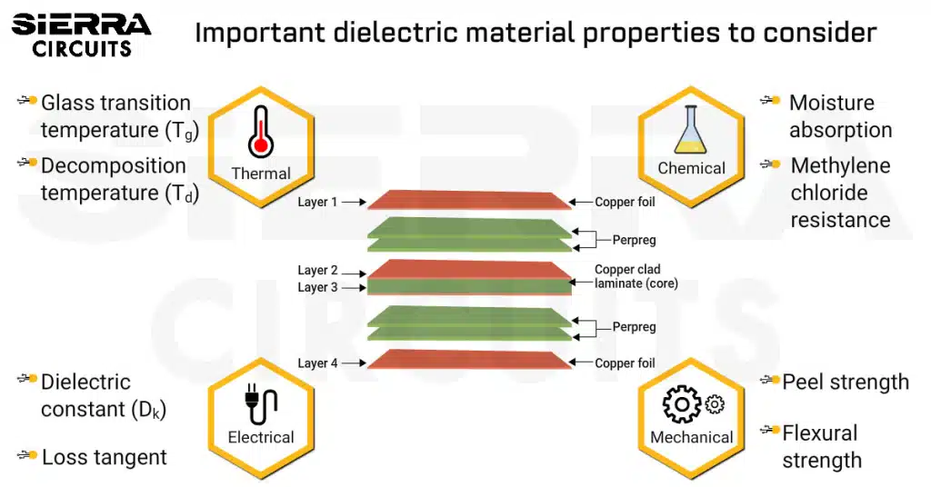
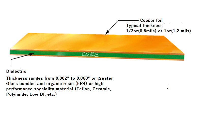
A PCB substrate is the dielectric material that electrically isolates copper layers in a multilayer stack-up. Besides insulation, it influences signal attenuation, crosstalk, impedance, and electromagnetic radiation, which directly affect signal integrity.
For example, a low-Dk material such as Rogers 4350B exhibits significantly lower high-frequency loss compared to a standard FR‑4 laminate.
In harsh environments such as aerospace or automotive systems, the PCB material must withstand high temperatures, humidity, and mechanical stress. Therefore, selecting the correct dielectric material is critical for reliability and performance.
In this article, we will discuss the electrical, mechanical, thermal, and chemical properties of a substrate, which will help you choose the right material for your design.
Highlights:
- A PCB substrate electrically isolates copper layers while influencing signal integrity, thermal performance, and mechanical reliability.
- Thermal properties such as Tg, Td, CTE, and thermal conductivity determine how the material behaves during soldering and high-temperature operation.
- Electrical properties such as dielectric constant and dissipation factor directly impact signal propagation, impedance control, and high-frequency losses.
- Chemical properties like moisture absorption and flammability ratings influence long-term reliability and environmental resistance.
- Mechanical properties such as peel strength, flexural strength, and time to delamination determine the structural integrity of the PCB.
What are the key thermal properties of PCB substrates?
Thermal properties that determine how materials behave under heat include glass transition temperature, decomposition temperature, coefficient of thermal expansion (CTE), and thermal conductivity (k).
1. Glass transition temperature (Tg)
Tg is the temperature range in which a PCB substrate transitions from a rigid glass-like state to a softer, more flexible state.
- Below Tg → material remains rigid
- Above Tg → polymer chains gain mobility and the material softens
When the temperature drops below Tg, the material returns to its original mechanical properties.
Typical glass transition temperature values for PCB laminates range from 130°C to 180°C, while high-performance materials may exceed 200°C.
2. Decomposition temperature (Td)
Td is the temperature at which a laminate chemically breaks down and loses at least 5% of its mass.
A substrate’s decomposition temperature is an important ceiling when assembling PCBs, because when a material reaches or surpasses its Td, changes to its properties are not reversible.
Contrast this to Tg, where properties will return to their original states once the material cools below the glass transition temperature range.
Choose a material where you can work in a temperature range that’s higher than Tg but well below Td. Most solder temperatures during PCB assembly are in the 200 ºC to 250 ºC range, so make sure decomposition temperature is higher than this (luckily, most materials have a Td greater than 320 ºC).
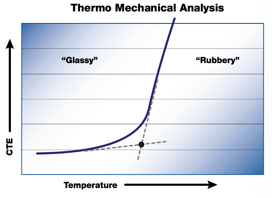
3. Coefficient of thermal expansion (CTE)
CTE describes how much a material expands when heated. It is measured in ppm/°C. As a material’s temperature rises past Tg, the coefficient of thermal expansion will rise as well.
The CTE of a PCB substrate is usually much higher than copper, which can cause interconnection issues as a PCB is heated.
CTE along the X and Y axes is generally low, around 10 to 20 ppm per degree Celsius. This is because the woven glass constrains the material in the X and Y directions, and the CTE doesn’t change much even as the material’s temperature increases above Tg.
So the material must expand in the Z direction. The CTE along the Z axis should be as low as possible; aim for less than 70 ppm per degree Celsius, and this will increase as a material surpasses Tg.
The point at which the displacement is maximum on the CTE curve is referred to as the glass transition temperature. If the temperature is higher than the Tg, the substrate softens and doesn’t expand any further.
4. Thermal conductivity (k)
It is a measure of how efficiently a material transfers heat. Low thermal conductivity means low heat transfer, while high conductivity means high heat transfer. The measure of the rate of heat transfer is expressed in watts per meter per degree Celsius (W/M -ºC).
Most PCB substrates have a thermal conductivity in the range of 0.3 to 0.6 W/M-ºC, which is quite low compared to copper, whose k is 386 W/M-ºC.
Therefore, more heat will be carried away quickly by copper plane layers in a PCB than by the dielectric material.
The table below outlines the key thermal properties of the substrate and their impact on performance.
| Property | Description | Why it matters |
|---|---|---|
| Glass transition temperature (Tg) | The temperature at which the laminate transitions from a rigid to a softened state | Higher Tg improves thermal stability during assembly |
| Decomposition temperature (Td) | The temperature at which the material chemically decomposes and loses mass | Must be significantly higher than soldering temperatures |
| Coefficient of thermal expansion (CTE) | The rate of expansion of the laminate when heated | Mismatch with copper can cause via failures |
| Thermal conductivity (k) | Ability of the material to conduct heat | Influences heat dissipation in high-power circuits |
Download the PCB Material Design Guide to learn how to pick the right laminates.

PCB Material Design Guide
9 Chapters - 30 Pages - 40 Minute ReadWhat's Inside:
- Basic properties of the dielectric material to be considered
- Signal loss in PCB substrates
- Copper foil selection
- Key considerations for choosing PCB materials
Download Now
What are the electrical properties of circuit board laminates?
Electrical characteristics affect how signals propagate, attenuate, and maintain integrity within a circuit board. Key parameters include dielectric constant (Dk), dissipation factor (Df), resistivity, and dielectric strength, which influence impedance, signal loss, and electrical insulation.
1. Dielectric constant or relative permittivity (Er or Dk )
The dielectric constant indicates how a material stores electrical energy and affects signal propagation speed. Typical PCB materials have Dk values between 2.5 and 4.5.
The dielectric constant varies with frequency and generally decreases as frequency increases; some materials have less of a change in relative permittivity than others.
Substrates suitable for high-frequency applications are those whose dielectric constant remains relatively the same over a wide frequency range, from a few 100MHz to several GHz.
Low Dk PCB materials
When a signal propagates through a substrate, its dielectric constant alters the signal behavior. This is because the EM wave emitted is not confined to the trace and passes through the substrate. This can cause severe signal integrity issues. This effect will be even more significant at high frequencies.
The speed of the propagating EM wave is inversely proportional to the dielectric constant. Hence, a low Dk PCB material will have the following advantages:
- High-speed signals propagate with lower losses
- Reduced crosstalk between closely spaced traces and vias
- Limits the need for capacitive coupling in the circuit
- Lowers the adverse effect of mismatched trace lengths in parallel nets
Even with all the advantages, the dispersion in the low Dk PCB material still exists, which can distort the digital signals. They are also more expensive than FR4. They may also need higher temperatures and pressure during the board fabrication process, which can drive the cost even higher. A few examples of high-speed materials include Rogers 4350B, RT Duroid 5880, and Isola-I speed.
High Dk board materials
Even though we associate power integrity with constant voltage input, the dielectric constant also affects the stability of the input power. If you place a high Dk material between the power and ground layers, the interplanar capacitance will become significant.
The planes themselves act as a large decoupling capacitor, which helps to maintain a constant input voltage. It also lowers the PDN impedance. However, a higher Dk will result in increased dielectric loss, crosstalk, and EMI issues. In order to balance power and signal integrity, it is advised to opt for a hybrid stack-up of high and low Dk PCB materials.
A higher dielectric constant substrate can be used for separating the power and ground layer, whereas the lower Dk substrate supports the signal layer with less loss. Manufacturing hybrid stack-ups depends on the manufacturer’s capabilities, as they have to consider the difference in CTE of the materials used.
2. Dielectric loss tangent or dissipation factor (Tan δ or Df )
A material’s loss tangent gives a measure of the power lost due to the material. The lower a material’s loss tangent, the less power is lost. The Tan δ of most PCB materials ranges from 0.02 for the most commonly used materials to 0.001 for very low-loss high-end materials.
It also varies with frequency, increasing as frequency increases. Read the difference between microstrip and stripline in PCBs.
Loss tangent isn’t usually a critical consideration for digital circuitry, except at very high frequencies above 1 GHz. However, it is a very important parameter for analog signals, as it determines the degree of signal attenuation and thus affects the signal-to-noise ratio at various points along signal traces.
The dielectric constant significantly impacts the controlled impedance and the width of the conductor. If the Dk is higher, then the trace width required will be lower to achieve the target impedance.
Low Df materials are essential for RF, microwave, and multi-GHz digital systems.
3. Volume resistivity (ρ)
Also known as electrical resistivity, it measures the insulation resistance through the material. The higher a material’s resistivity, the less readily it allows the movement of electric charge, and vice versa. Resistivity is expressed in ohm-meters (Ω-m) or ohm-centimeters (Ω-cm)
As dielectric insulators, circuit board substrates are required to have very high values of resistivity, in the order of 10⁶ – 10¹⁰ Megaohm-centimeters. Resistivity is somewhat affected by moisture and temperature.
High resistivity ensures the substrate does not allow unwanted current leakage.
4. Surface resistivity (ρS)
It is the measure of the electrical or insulation resistance of the surface of a circuit board substrate. Like volume resistivity, PCB materials are required to have very high values of surface resistivity, in the order of 10⁶-10¹⁰ Megaohms per square. It is also somewhat affected by both moisture and temperature.
5. Electrical strength
Electrical strength measures a PCB substrate’s ability to resist electrical breakdown in the PCB’s Z direction (perpendicular to the PCB’s plane). It is expressed in Volts/mil. Typical electrical strength values for PCB dielectrics are in the range of 800 V/mil to 1500 V/mil.
Electrical strength is determined by subjecting the PCB material to short high-voltage pulses at standard AC power frequencies.
| Property | Description | Typical range |
|---|---|---|
| Dielectric constant | Measures the material’s ability to store electrical energy. Higher Dk slows signal propagation and lowers impedance. | 2.5-4.5 |
| Dissipation factor | Also known as loss tangent; represents signal energy lost as heat within the substrate. | 0.001-0.02 |
| Volume resistivity | The electrical resistance through the bulk of the dielectric material. | 106-1010 MΩ-cm |
| Surface resistivity | The electrical resistance along the surface of the insulator. | 106-1010 MΩ/sq |
| Dielectric strength | The maximum electric field the material can withstand before electrical breakdown occurs. | 800-1500 V/mil |
Sierra Circuits manufactures and assembles high-quality standard and advanced circuit boards.
Talk to a PCB expert: Book a meeting or call us at +1 (800) 763-7503.
What chemical properties influence PCB substrate reliability?
Factors such as flammability rating, moisture absorption, and chemical resistance determine how the material performs under environmental exposure.
1. Flammability specs (UL94)
UL94, or the Standard for Safety of Flammability of Plastic Materials for Parts in Devices and Appliances testing, is a plastics flammability standard that classifies plastics from lowest (least flame-retardant) to highest (most flame-retardant).
The standards are defined by Underwriters Laboratories (UL). Most PCB substrates adhere to UL94 V-0; here are its requirements
- The specimens may not burn with flaming combustion for more than 10 seconds after either application of the test flame.
- The total flaming combustion time may not exceed 50 seconds for the 10 flame applications for each set of 5 specimens.
- The specimens may not burn with flaming or glowing combustion up to the holding clamp.
- The specimens may not drip flaming particles that ignite the dry absorbent surgical cotton located 300 mm below the test specimen.
- The specimens may not have glowing combustion that persists for more than 30 seconds after the second removal of the test flame.
2. Moisture absorption
It is the ability of a board substrate to resist water absorption when immersed in water. It is given by a percentage increase in the weight of a PCB material due to water absorption under controlled conditions as per standard test methods. Most substrates have moisture absorption values in the range of 0.01% to 0.20%.
Moisture absorption affects the thermal and electrical properties of the substrate, as well as the ability of the material to resist conductive anode filament (CAF) formation when a PCB is powered on. For high-speed designs, laminates are often baked before lamination to remove absorbed moisture.
3. Methylene chloride resistance
It is a measure of a material’s chemical resistance; specifically, the ability of a PCB material to resist methylene chloride absorption.
Just like moisture absorption, it is expressed by a percentage increase in the weight of a PCB material due to exposure to or soaking in methylene chloride under controlled conditions. Most PCB materials have methylene chloride resistance values in the range of 0.01% to 0.20%. Lower values indicate better chemical resistance.
To learn how to pick the right substrates, download the High-Speed Material Design Guide.
High-Speed Material Design Guide
6 Chapters - 19 Pages - 30 Minute ReadWhat's Inside:
- Importance of choosing the right material for your high-speed design
- Parameters that affect material selection
- Effect of dielectric constituents on your circuit board
- Characteristics of high-speed materials
- Effect of resin content and glass weave structure on your PCB
Download Now
Effects of moisture absorption on dielectric constant
Michael J. Gay, Director, High-Performance Products, Isola Group, stated that “Moisture is one of the sources of Dk variation in PCB materials. There are other possible sources that could potentially result in some minor variation, but moisture uptake over time is a fairly large potential factor.” The chart below shows the moisture uptake in a 24-hour DI water soak at various temperatures for Tachyon 100G material.”
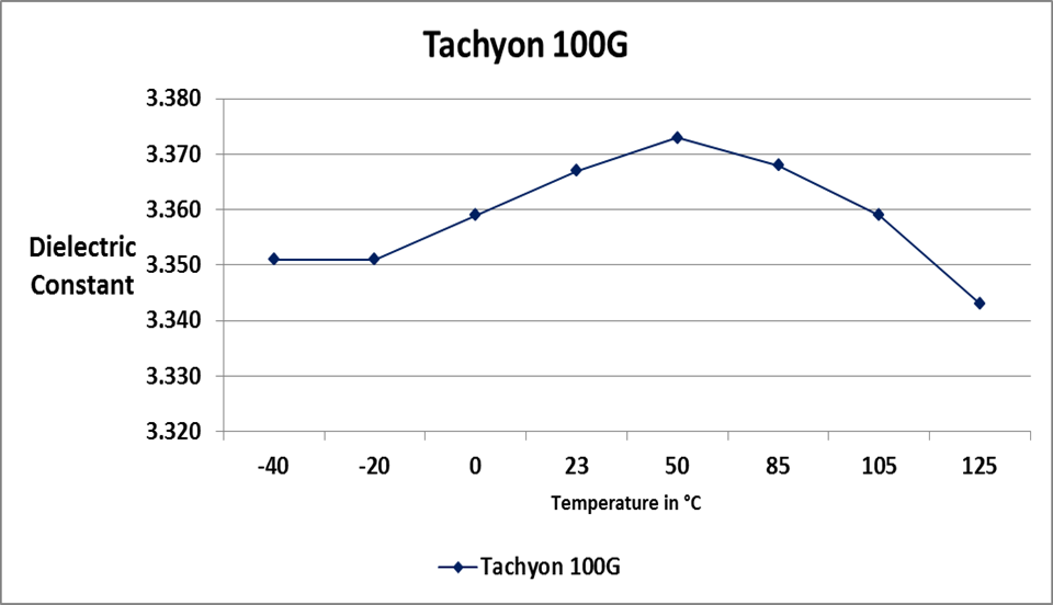
Michael further explained, “As you can see, the Dk is about 0.02 higher after the material becomes saturated at 23 °C or room temperature. It is not a huge difference, but it might make you think of changing the line width requirement to center the impedance. Moisture uptake would happen to the clad laminate over many weeks or to the etched laminate over several hours. Uptake is dependent on the length of the path for the material to reach equilibrium. For example, a single etched signal layer core sitting in AOI for a few hours would pick up the maximum moisture content at RT (relative temperature). These areas are usually about 60% RH (relative humidity), and so moisture is readily available.”
In an actual PCB design, the moisture may not stay in the areas near hot components and be driven out of the board when temperatures reach 80-90 °C near hot chips.
Test methodology
- The sample was pulled from the water soak and then equilibrated for 4 hours before the -40 °C reading.
- Each subsequent reading was taken after an equilibration of 150 minutes at a new temperature.
Key takeaways of the experiment:
- Dk response as expected: It increases as water transitions through phases and then decreases as moisture is driven off from the sample.
- Df response is also as expected: A slow increase in loss due to the same phase transitions in the retained moisture, followed by a decrease as the moisture is driven off.
- Additional testing could be supported with different test conditions.
Michael also likes to add, “For high-speed design, we recommend that materials are dry prior to lamination using a baking process. In materials like Tachyon 100G, moisture does not negatively influence curing, but as you can see, moisture does result in Dk shifting.”
For conveyorized oxide replacements, an efficient dryer at the end of a conveyorized oxide replacement line should remove all moisture from the inner layer surface. However, drying on layers for 30 minutes at 100°C or higher is considered a best practice, especially for the boards subjected to lead-free processes. Drying in racks is preferred.
For other materials, especially epoxy-based resin systems, moisture can also impede the cure reaction and result in lower thermal resistance and thermal properties. We recommend baking the inner layers to avoid this problem.
On the finished board of all materials, you will see a similar variation in Dk if the boards are not dry. All polymeric materials pick up moisture. The reason that moisture causes problems is that it is a polar molecule and interferes with the magnetic fields in the local vicinity. This is the very reason why some resins are higher loss, and some are lower loss – polarity of the resin molecules. For instance, PTFE is a very low-polarity resin and is a low-loss material.
Michael concluded, “Moisture can easily find its way through the resin molecules and park between them because it is so small. The amount of water a plastic can absorb is a result of the amount of free space in the cured resin. Some have more free space than others.”
Visit our rigid PCB manufacturing capabilities to learn more.
What are the mechanical properties of circuit board materials?
Parameters such as peel strength, flexural strength, Young’s modulus, and time to delamination indicate the substrate’s ability to withstand mechanical and thermal stress.
1. Peel strength
It is a measure of the bond strength between the copper conductor and the dielectric material. It is expressed in pounds of force per linear inch (PLI, or average load per conductor width) required to separate bonded materials where the angle of separation is 180 degrees.
Peel strength tests are done on samples of copper traces of 1 OZ thick and ~ 32 to 125 millimeters wide after standard PCB manufacturing processes. It is completed under 3 conditions:
• After thermal stress: after a sample is floated on solder at 288 ºC for 10 seconds
• At elevated temperatures: after a sample is exposed to hot air or fluid at 125 ºC
• After exposure to process chemicals: after a sample is exposed to a specified series of steps in a chemical or thermal process
2. Flexural strength
It is the measure of a material’s capability to withstand mechanical stress without fracturing. It is expressed in either Kg per square meter or pounds per square inch (KPSI).
Flexural strength is generally tested by supporting a PCB at its ends and loading it in the center. IPC-4101 is the Specification for Base Materials for Rigid and Multilayer Printed Boards, and it gives the minimum flexural strength of various PCB materials.
3. Young’s modulus
Also known as tensile modulus, it measures the strength of a PCB material. It is the stress/strain ratio in a particular direction, and some PCB laminate manufacturers give strength in terms of Young’s modulus instead of flexural strength. Like flexural strength, it is expressed in force per unit area. Higher values indicate a stiffer material.
Some PCB laminate manufacturers give the PCB materials strength not in terms of Flexural Strength but in terms of Young’s modulus, which is a measure of stress/strain ratio in a particular direction.
4. Density
The density of a PCB material is expressed in grams per cubic centimeter (g/cc) or pounds per cubic inch (lb/in^3).
5. Time to delamination
It is a measure of how long a material will resist delamination, the resin’s separation from the laminate, foil, or fiberglass, at a specified temperature. Delamination can be caused by thermal shock, the wrong Tg in the material, moisture, and a poor lamination process.
To quickly select the best material, use the Sierra Circuits Material Selector tool. Input a specific material property or properties, and the tool will give you a list of high and low Dk PCB materials that meet your requirements.

The tool also provides an easy-to-use comparison table that lets you compare the detailed properties of 50+ rigid and 10+ flex materials.
To learn more about PCB material selection, watch our webinar PCB Material Selection: Electrical and Manufacturing Considerations.
About the author: Atar Mittal is the Director and General Manager of the design and assembly division at Sierra Circuits. He is responsible for the design and development of strategies and process automation tools for complex printed circuit boards and assemblies. Atar is also currently engaged in the development of productivity tools for electronics designers that would have a tremendous impact on shortening the development time.
Need assistance in selecting the right material for your circuit board? Post your queries on our PCB forum, SierraConnect. Our design and manufacturing experts will help you select one.

About Atar Mittal : Atar Mittal is the General Manager and Director of the Design and Assembly Sierra Circuits division. He has a degree in Electrical Engineering from IIT Kharagpur and has worked in the electronics industry for over three decades.


Start the discussion at sierraconnect.protoexpress.com