


Contents
Low-power, high-performance circuits are often plagued by power supply-related issues. This common occurrence is frequently due to mythical (or misapplied) rules of thumb.
These rules of thumb often lead us in the wrong direction, making things worse rather than better. In this article, I’ll highlight some of the most common mistakes engineers make and share some fundamental rules for designing clean power for sensitive circuits. Applying these rules will result in higher performance and lower cost designs with fewer design iterations.
What is a sensitive circuit?
Sensitive circuits are those that can easily be degraded by power supply noise. These circuits generally include oscillators, LNAs, transceivers, mixers and ADCs. I’ll probably receive emails from many readers adding to my list, and justifiably so, so take these as a few examples and not a comprehensive list.
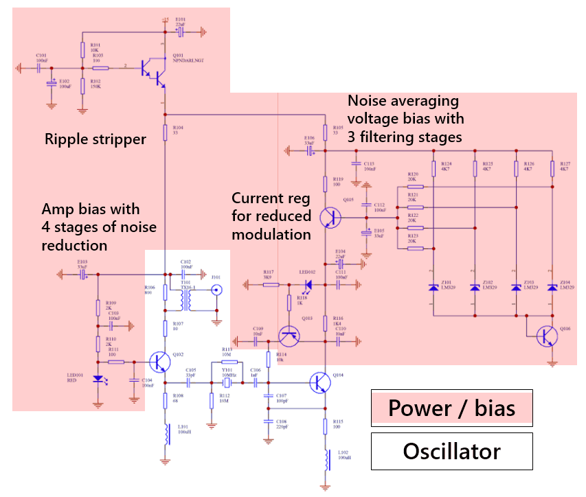
Experienced oscillator designers are well aware of the challenges related to the power supply. This is clearly evident in the oscillator schematic shown in Fig. 1. Approximately 75% of the components in this design are related to the power supply while 25% of the components are related to the oscillator.
What is the sensitive circuit sensitive to?
The obvious answer is that the circuit is sensitive to power supply noise, right? The oscillator circuit in Fig. 1 can be represented as a circuit with just two connections (or ports for RF guys) – the power supply input and the oscillator output, so you might jump to the conclusion that the noise is obviously generated by the power supply.

RF & Microwave Design Guide
8 Chapters - 44 Pages - 60 Minute ReadWhat's Inside:
- Basics of RF and microwave board design
- Choosing RF materials
- Trace, grounding, via, and stack-up design
- Component selection and placement
- Testing and isolation requirements to avoid interference
Download Now
And this obvious conclusion is the reason for the most common mistakes engineers make when designing power for sensitive circuits. Two more important questions are where does the noise come from and how does it get there?
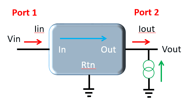
The power supply can also be viewed as a circuit with just two connections (or ports) – The input to the power supply and the output from the power supply. This simplistic view, shown in Fig. 2, is valid independent of whether the power supply includes a voltage regulator, a passive noise filter, or just a wire connected between the power supply input and output.
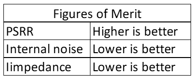
The noise at the output of the power supply is a summation of independent noise sources flowing to the output through different paths. For example, voltage noise present at the power supply input flows through to the output. This path is defined as Power Supply Rejection Ratio or PSRR.
A figure of merit for the power supply is, therefore, PSRR and higher PSRR performance results in less input noise appearing at the power supply output. Noise is also generated internal to the power supply.
In the case of a switching regulator, this is clear, but even linear regulators generate noise and not all regulators are created equal. A second figure of merit is, therefore, the self-generated power supply noise. For tips on power supply, read 7 considerations for PCB power supply design.
A third noise path is the result of the power supply presenting a finite, non-zero output impedance. Current variations at the power supply output, are multiplied by the power supply impedance, resulting in power supply output voltage noise.
These current perturbations can be generated by the sensitive load circuitry, by other circuits sharing the power supply output, or even due to radiated electromagnetic fields coupling into the power supply output. This leads to a third figure of merit; the output impedance of the power supply.
The noise at the output of the power supply is quantified as the summation of the noise from these three independent paths.

From the previous discussion and equation 1, we can summarize three power supply figures of merit for powering sensitive circuits, though these figures of merit apply quite broadly to other circuits as well.
Common mistakes engineers make while designing a power supply
Solving (1) requires at least three pieces of data:
- The impact of power supply noise on the performance of the sensitive circuit
- Noise current presented by the sensitive circuit.
- The impedance of the sensitive circuit

The most common mistake is designing the power supply without these three pieces of data. One reason this is the most common is that despite this information being critical it’s rarely (if ever) provided as part of the circuit specification or datasheet and, therefore, requires the designer to perform the measurement. Obtaining this data is essential to designing a cost-effective, suitable power supply.
Need help in designing reliable high-power PCBs? Our engineering team can help you with thermal management, stack-up design, and DFM analysis.
You can book a meeting with our experts or call us at +1 (800) 763-7503.

A Clear Path to Victory
Don’t do anything else until you have obtained or measured the sensitivity of the sensitive circuit to power supply noise. This generally involves connecting a Line Injector device (https://www.picotest.com/products_J2120A.html) between a clean bench power supply and the sensitive circuit.
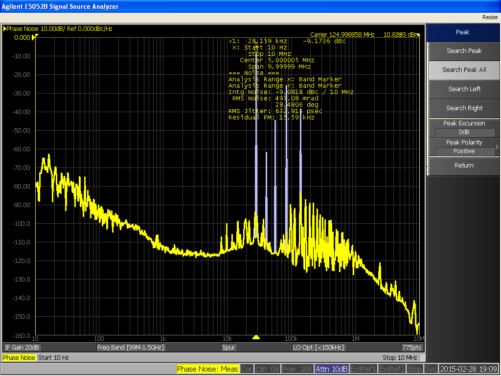
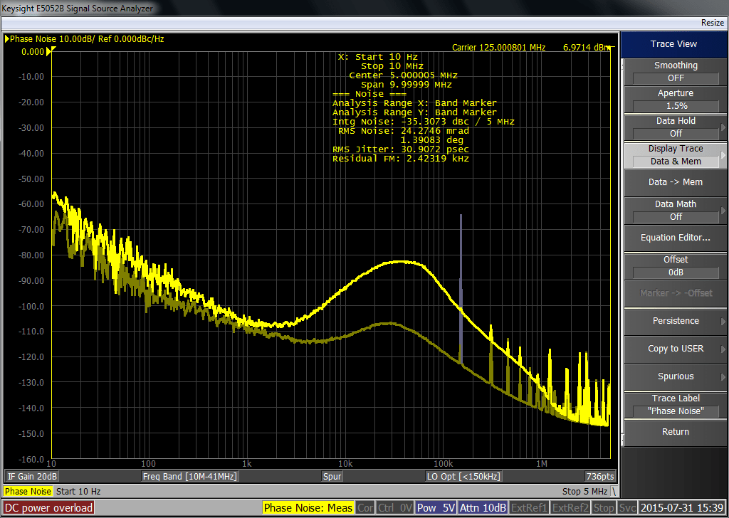
The line injector is modulated while monitoring the output of the sensitive circuit, an oscillator in the example shown in Fig. 3. The power supply is modulated by a 20mV, 28kHz sine wave. The measurement shows the noise spur in the oscillator output resulting from the power supply modulation signal, as well as some of the harmonics of the modulation signal.
This process of modulating the power supply and monitoring the resulting spur is repeated at many frequencies and the results are tabulated and graphed as shown in Fig. 4.
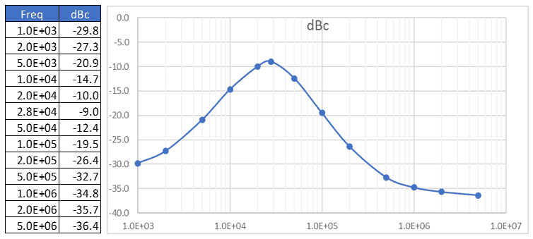
The graph in Fig. 4 shows that the oscillator being measured is most sensitive to power supply noise at 30kHz. This response is typical of a phase lock loop (PLL) internal to the oscillator. The frequency of maximum sensitivity is a function of the PLL circuit design and can be anywhere from a few kHz to tens of MHz.
The spur amplitude in Fig. 3 is approximately 100dB, extending from approximately -110dBc to the peak of -9dBc. Allowing 3dB degradation due to power supply noise the power supply noise density at 28kHz is limited to a maximum of:
![]()
The same procedure can be used to determine the power supply noise density at many other frequencies thereby providing a frequency related noise budget. Substituting into (1) allows the noise to be allocated among the three noise sources.
![]()
The measured phase noise plot in Fig. 5 shows the result of a low noise low impedance linear regulator powering the oscillator directly and through a 2Ω series resistor. In this case the difference between these two curves at 28kHz is approximately 26dB. Again, allowing 3dB degradation results in a maximum power supply impedance of:
![]()
And the minimum PSRR is determined from the maximum noise at the input to the power supply as:
![]()
Exceeding these requirements by more than a few dB won’t provide much in the way of performance improvement and so wouldn’t justify a more expensive power supply.
The third common faux pas is (inappropriately) adding ferrite beads and ceramic capacitors to filter the noise or correct the deficiencies resulting from the first two mistakes above. It’s important to assess the input impedance of the sensitive circuit since often there are ceramic capacitors internal to the sensitive circuit.
Ferrite beads can be quite inductive at low frequencies raising the impedance of the power supply and, therefore, require capacitance to counteract the inductance. The capacitance required can be determined from the value of the bead inductance and the output impedance calculated in (4) above. For example, using a bead that presents an inductance of 2uH:
![]()
And the ESR of the capacitor should be approximately equal to the resistance calculated in (4) and so for this example:
![]()
Note that the required capacitance can be quite large. Reducing the ESR and/or the capacitance will result in an impedance resonance and degraded circuit performance. A final consideration is that the ESL of this filter capacitor can resonate with any ceramic capacitance internal to the sensitive circuit. Assuming a filter capacitor ESL of 2nH (reasonable guess for an electrolytic capacitor), then maintaining low Q to avoid an impedance resonance, requires that the ceramic capacitance be:
![]()
Again, optimum performance is achieved if this ceramic capacitor has an ESR of 0.14Ω consistent with (4) and (7). This may require an external series resistor or an ESR controlled ceramic capacitor.

Designing an optimum power supply for sensitive circuits is simple if you follow the three steps I’ve outlined here.
First, obtain the data for the power supply sensitivity for your circuit. This often means acquiring the data yourself or asking your supplier to provide it in a form similar to what I’ve shown here.
Second, use measurements to determine the sensitivity of the circuit to power supply resistance.
Third, make sure you know the impedance presented at the power supply input to the circuit.

References:
- S. M. Sandler, Clock Power Optimization Depends On Jitter Control, Electronic Design Sept. 9, 2012 www.electronicdesign.com/analog/clock-power-optimization-depends-jitter-control
- S. M. Sandler, Troubleshooting Clock Jitter and Identifying PDN sensitivities, EEWeb Apr. 11, 2016 www.eeweb.com/blog/eeweb/troubleshooting-clock-jitter-and-identifying-pdn-sensitivities
- Keysight How to Design for Power Integrity YouTube video series www.keysight.com/find/how-to-videos-for-pi
- Troubleshooting Clock Jitter, Keysight Solution Brochure http://literature.cdn.keysight.com/litweb/pdf/5992-1645EN.pdf?id=2767985
- Low Phase Noise Design: Crystal Oscillators http://www.ko4bb.com/~bruce/CrystalOscillators.html


