Contents

On-demand webinar
How Good is My Shield? An Introduction to Transfer Impedance and Shielding Effectiveness
by Karen Burnham
Ethan Pierce, Director of Hardware Engineering at Pierce Design, offered valuable insights into the evolving trends and IoT PCB design challenges.
Highlights:
- New sensors, cutting-edge interface paradigms, and advanced board materials are a few of the emerging trends in the IoT industry.
- When positioning sensors on your board layout, make sure to provide a reference plane beneath the device to minimize interference and EMI.
- Include multiple footprints for components like microcontrollers or FPGAs in your design
- Siemens Expedition is the go-to tool for mil/aero, while Altium Designer is popular in industries like the automotive and telecommunication sectors.
Watch the full video to learn more:
What are the new trends in the IoT industry that a PCB designer should know?
Ethan Pierce: In the IoT industry, it’s crucial for PCB designers to stay updated with the latest developments. New sensors, advanced board materials, and interface paradigms are consistently emerging. You need to keep exploring new technologies, materials, and component packages. These factors will play a significant role as your organizations and teams work on creating connected products, whether they’re 5G devices, autonomous vehicles, or embedded wearable tech.
It’s vital to recognize that technology keeps advancing, so staying informed about new vendor materials and their impact on PCB designs is essential.
To learn how to design 5G-enabled IoT devices, read antenna integration and RF design guidelines for 5G PCBs.
What are the key factors to consider when integrating sensors into PCB layouts?
Ethan Pierce: When integrating a sensor into a circuit board design, several critical considerations come into play. One important factor is the placement of the sensor. It’s essential to ensure that the area beneath the sensor, where the signal traces emerge from the package, includes a reference plane. Without a reference plane beneath these signals, the electromagnetic waves they generate might interfere with other components. Further, it can potentially lead to crosstalk and impact nearby sensors. Therefore, it’s crucial to have a well-defined reference plane beneath all your signals. This is essential to maintain signal integrity and prevent unwanted interference.
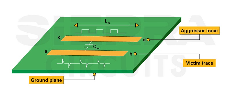
Always collaborate with your product design team when deciding on sensor placement. This collaboration is essential to finalize whether you’re implementing central computing with sensors near the PCB or positioning them a few inches away.
If you choose to place sensors at a distance from the circuit board, you need to consider whether you’ll be routing analog traces or digital signals back to the computing system.
Various factors will influence your decision. This includes the mechanical structures involved, the preferences of your product design teams, the materials used, and the type of application (static or exposed to external conditions).
It’s crucial to keep these aspects in mind as PCB design interfaces with mechanical engineering, software engineering, and electrical engineering. A well-coordinated effort among these disciplines is essential during the board’s design process.
Learn what Rick Hartley has to say about PCB design recommendations to minimize EMI.

Signal Integrity eBook
6 Chapters - 53 Pages - 60 Minute ReadWhat's Inside:
- Impedance discontinuities
- Crosstalk
- Reflections, ringing, overshoot and undershoot
- Via stubs
Download Now
What are some common design pitfalls to avoid when designing PCBs for IoT applications?
Ethan Pierce: Typically, in IoT application designs, people sometimes skip the important step of collaborating with their vendors and conducting tests before moving into production. There are instances where a component is chosen, but it later becomes unavailable or fails to meet the necessary requirements.
It’s crucial to take steps to reduce risks during the design phase. This is especially important in your proof of concept and prototype stages. Instead, commit to a particular sensor or any component in your IoT design only after ensuring that all aspects work well. It’s wise to validate that the entire system is functional, scalable, and stable before moving into full-scale manufacturing.
When designing PCBs for IoT applications, what factors do you prioritize to ensure low power consumption and extended battery life?
Ethan Pierce: I’ve certainly learned this lesson the hard way before. When working on your IoT design, it’s essential to consider the device’s expected lifespan in the field.
Furthermore, you should take into account the usage cycle of the device. Will users bring the device back for recharging or maintenance? How will they replace the power system and batteries? Once you have these details, you can make informed component selections. Factors like leakage current and the various stages with your regulators become crucial. Keep in mind that every time you pass through a switching regulator stage, you’ll experience some efficiency and power loss.
It’s vital to consider the thermal aspects of your design. Conducting a circuit board thermal analysis is key. Understand where the device will be located and how much power it will generate. This becomes especially crucial with technologies like ultra-wideband, where transmitters often need to be active and consume a significant amount of power.
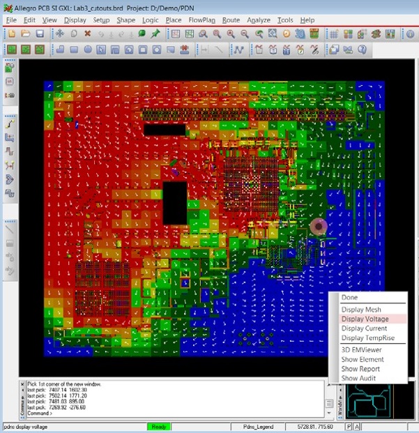
Furthermore, it’s crucial to think about power management and component selection. As a designer, collaborate with electrical engineers to ensure that integrated components can enter power states when necessary. Make sure there’s accurate circuitry to support this. Additionally, ensure there’s enough copper underneath the components, and avoid using excessively thin traces, particularly for analog signals.
Ultimately, a deep dive into the data sheets and thorough testing of your devices is essential. This will determine whether your device meets the longevity requirements for field use based on your design specifications.
For circuit board heat dissipation techniques, see 12 PCB thermal management techniques to reduce PCB heating.
How do you deal with miniaturization challenges when designing PCBs for compact IoT devices and medical implants?
Ethan Pierce: One of the major IoT PCB design challenges is miniaturization. I’ve given this a lot of thought, and one thing to keep in mind as a designer is that you can’t possibly know everything. What’s crucial when dealing with miniaturization is to understand the design principles and technologies your organization relies on. Then, based on the requirements of the next generation of products, work closely with various vendors and manufacturers. This includes component suppliers and fabricators.
As new technologies emerge, you may encounter challenges. In such cases, don’t hesitate to engage with your fabricator. For instance, you might need to implement a process that involves creating one-mil traces in tight spaces. Fortunately, there are new vendors and fabricators that specialize in additive processes for achieving miniaturization. The key is to maintain open communication with your fabricator and vendors while safeguarding any proprietary information. Due diligence is essential in ensuring a successful design.
To sum it up, having a foundational level of knowledge is crucial. Collaborate with your community of vendors and partners to collectively achieve the miniaturization objectives your team has set.
To learn how to design compact boards for 5G-enabled IoT devices, see How to design a PCB for 5G wireless applications.
IoT solutions often need to scale as more devices are added to a network. How do you design PCBs with scalability in mind to accommodate future growth?
Ethan Pierce: When considering scalability for an IoT device, it’s crucial to take modularity into account. Think about the number of devices deployed and their expected lifespans. In my experience, building an IoT device involves modularity not only in terms of using interchangeable modules for connectivity but also in the design itself.
Given the silicon shortage and the need for scaling, it’s beneficial to include multiple footprints for components like microcontrollers or FPGAs in your design. This allows flexibility to accommodate parts from different manufacturers that serve the same purpose and facilitates scalability.
What would you advise aspiring PCB designers aiming to excel in IoT, medical, and defense applications?
Ethan Pierce: To excel in these fields, continuous learning and networking are key. Don’t stay isolated; connect with fellow designers and professionals. Ask your manager about opportunities to attend conferences like PCB West, which offers a wealth of technical content. Engage with fabricators to stay updated on new technologies and advancements.
Collaborate, learn from research papers, attend conferences, or simply have casual discussions. Networking and staying open to new ideas are how you’ll be able to take your career to the next level.
What tools and software do you prefer for IoT PCB design, and why?
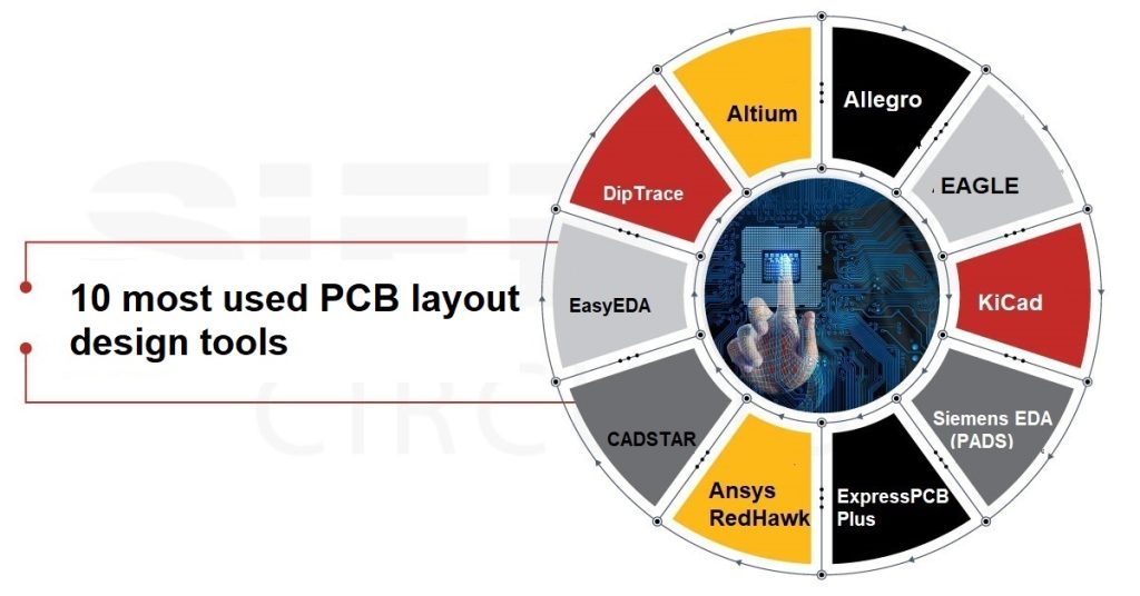
Ethan Pierce: The choice of PCB design tools is often a hotly debated topic. It’s my strong belief that if you’re an IoT company building open-source products, it’s crucial to align your design with an open-source toolchain. KiCad is a widely available choice in this regard.
For many enterprise companies, Altium Designer is the tool of choice, while industries with more complex mil/aero needs, like aerospace and defense, often opt for Siemens Expedition. Currently, we’re facing a workforce crunch with many experienced designers retiring or leaving the industry, leaving a significant void for new designers. To bridge this gap, it’s important to remain flexible and open to using a variety of tools.
KiCad Design Guide
10 Chapters - 161 Pages - 180 Minute ReadWhat's Inside:
- Creating a component symbol library
- Setting up board parameters and rules
- How to route differential pairs
- How to place of components
Download Now
If you’re looking to get a jumpstart in PCB design, Altium Designer is an excellent choice. It provides an opportunity to gain expertise in the toolset commonly used in enterprise applications.
Fusion 360 with Fusion Electronics is ideal for hobbyist designs, effectively replacing what Eagle used to do before Autodesk integrated it. Additionally, it’s important to acknowledge Orcad and Allegro from Cadence, which are widely popular in various industries, particularly in the smartphone industry. Many organizations have built their workflows, scripts, and processes around these tools, making them essential for iterative product development. Hence, they are not moving away from these tools anytime soon.
Moreover, even in the consumer and general commercial fields, you might come across tools like OrCAD and Allegro, as they are frequently used options. Understanding the specific industry you’re targeting will help you make an informed decision about which PCB design software to focus on.
As a designer working on IoT applications, you might already be familiar with the use of large language models like OpenAI’s ChatGPT. While you don’t have to rely exclusively on these tools, I’ve personally found them to be incredibly beneficial in speeding up my workflow. They’re handy for tasks such as handling data sheets, user guides, and even software development. These AI tools are becoming increasingly powerful.
While AI tools for layout are still in their early stages, there are companies like Circuit Mine that offer the capability to create schematics from a block diagram and seamlessly integrate them into software like Altium for component placement. It’s vital to keep an eye on emerging trends in AI tools. This especially includes trends related to large language models, as they can significantly enhance your design process.
Here’s an overview of the 10 most used PCB layout design tools.
Key takeaways:
- Sensors should have a reference plane beneath them to avoid signal integrity issues.
- Avoid common design pitfalls by collaborating with vendors, conducting tests, and choosing components that best suit your application.
- Design IoT PCBs with scalability in mind. Incorporate modularity and multiple component footprints to accommodate future growth.
- Altium Designer is an excellent choice for gaining expertise in PCB design, especially for enterprise applications.
- Fusion 360 is ideal for hobbyist designers.
- Orcad and Allegro from Cadence are widely popular tools, particularly in the smartphone industry, and many organizations rely on them for iterative product development.
Incorporate these design guidelines from Ethan Pierce into your next project. His insights will assist you in overcoming common IoT PCB design challenges and provide a valuable roadmap for navigating the dynamic landscape of connected devices.
If you have any design queries, please feel free to post them on our PCB forum, SierraConnect and get them answered by industry experts.
About Pooja Mitra : Pooja Mitra is an electronics and communication engineer. With an experience of over three years in the PCB industry, she creates industry-focused articles that help electrical and PCB layout engineers.




Start the discussion at sierraconnect.protoexpress.com