Contents

On-demand webinar
How Good is My Shield? An Introduction to Transfer Impedance and Shielding Effectiveness
by Karen Burnham
Combining flex and HDI PCB technologies can ensure that the circuit boards powering the IoT are sufficiently small and high-performing to power a wide variety of devices. They can help drive down the number of wiring connectors, minimize space and weight, and improve PCB reliability through the reduction of things such as thermal stress.
Several big trends have converged to make the Internet of Things possible:
- Wireless networking technologies such as Wi-Fi and 4G LTE have continually improved and become viable alternatives to wired connections like Ethernet.
- Devices such as the Nest thermostat and the Philips Hue lightbulbs have demonstrated how connectivity can be extended to many new and more compact device types. Smartphones were one of the first usable ways to access the Internet without having to rely on a laptop or desktop. Now applications can be pulled up from a smartwatch or deeply woven into the activities of connected home appliances.
- Printed electronics have evolved to become flexible and suitable for a variety of form factors. The IoT PCB design requirements for flex and High-Density Interconnect (HDI) boards enable the manufacturing of sophisticated wearables ranging from medical implants and hearing aids to fitness trackers and augmented reality heads-up displays. These boards provide excellent design freedom (i.e., they can be formed into many shapes), high copper tensile strength, and are suitable for harsh environments.
These three trends have enabled the IoT and also driven up demand for flex and HDI PCBs in particular. Let’s look at bit more in depth about why these types of PCBs will play a central part in the IoT.
What are the IoT opportunities for Flex and HDI PCB Design?
Tens of billions of new devices will be connected to IP networks as the IoT spreads, and many of them will need PCBs that can fit into tight spaces while still delivering high performance. IT research firm Gartner has estimated that by 2020, up to 26 billion devices could be connected to the Internet.
HDI PCB Design Guide
5 Chapters - 52 Pages - 60 Minute ReadWhat's Inside:
- Planning your stack-up and microvia structure
- Choosing the right materials
- Signal integrity and controlled impedance in HDI
- Manufacturing considerations for higher yields
Download Now
Providing flexibility for wearable applications
Applications for IoT devices such as wearables put unique demands on PCBs. For example, a circuit board within a fitness tracker would likely be subject to frequent flexing and other forms of dynamic stress. Device makers have responded by exploring options like flex PCBs and HDI PCBs.
One specific approach, described in the June 2015 of The PCB Magazine, would be to connect multiple PCBs by using elastic copper conductors. Each board would have its own surface mount components, while the entire creation would be contained within an elastomeric material to ensure a stretchable system.
This level of flexibility builds on the potential already demonstrated by flex PCBs in applications such as medical devices, aerospace equipment, and cars. With something like a hearing aid, a flex PCB enables components such as batteries, microphones, and digital signal processors to be mounted in one small package. In a car, a flex PCB can greatly simplify an otherwise complicated wiring harness and also provide effective resistance within the harsh environment under the hood.
Where HDI fits into the IoT
HDI allows for dense component placement and more versatile routing in a PCB. The main benefit of HDI is that it reduces drill to copper. Using blind and buried vias allows designers to avoid denser areas of the board, which in turn means the denser circuitry is routed cleaner.
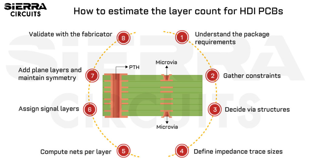
Compared with traditional PCBs, HDI PCBs have tinier trace widths and superior wiring density. They achieve these advantages through the use of technologies such as buried vias, blind vias, and stacked microvias.
Another note on microvias: Their extremely small pad size, as described in a 2014 EE Times article by Pi Zhang of Nuvation Engineering, helps to boost channel routing width. Layer reduction is possible since through-holes may be replaced with microvias, allowing signal layers along with their corresponding reference planes to be eliminated. It’s the PCB version of hitting two birds with one stone.
Also read: Happy Holden Discusses HDI
What are the IoT opportunities for PCB Design?
The Internet of Things is poised to grow and evolve rapidly in the coming years, and businesses eager to take advantage of these trends need to take action as quickly as possible.
Of course, speed is only part of the equation.
In order to truly thrive in the IoT space, companies must also ensure their applications are designed to meet all of the IoT’s various intricacies. With that in mind, here are a few of the most important design requirements to make note of while developing solutions for the IoT:
Purpose
The IoT industry is complex, wide-ranging, and ever-changing. It’s easy for IoT application developers to overlook one of the most critical IoT objectives: Every IoT-related solution needs to fulfill a specific purpose and address a clear problem.
“Keeping the solution’s purpose in mind through every design stage will be critical.”
This doesn’t always happen. Consider Revolv, developed by Nest. Nest is intricately tied to the IoT, as its sensor-driven thermostat systems are among the most popular consumer-facing examples of the IoT on the market. However, the Revolv was neither profitable or a success by any means. This product served as a home automation hub that could interact with everything from entertainment systems to light switches to garage doors, but as Harvard Business Review contributors Scott A. Nelson and Paul Metaxatos noted, this range of services didn’t come together to actually address any customer needs. As a result, there was little demand for the product.
IoT companies need to avoid falling into this trap. To that end, keeping the solution’s purpose in mind through every stage of the design process will be critical.
Size and IoT
The IoT is vast, incorporating a huge range of possible applications. Ultimately, though, the vast majority of applications share one trait in common: They’re small. From smart thermostats to data-gathering machine sensors in manufacturing plants to wearables, most IoT applications are tiny by necessity. As businesses look to further leverage the IoT for different purposes, this physical limitation isn’t going away. As such, any IoT application design needs to factor in size early on.
Reliability in IoT
Reliability is critical for IoT application designs for two reasons. First, there are many instances where the sensors and other solutions will be difficult to access, as is the case for a device that improves deep-sea drilling through the detection of ocean currents. Considering the challenges in repairing or completely replacing these IoT devices, companies are going to be insistent on a high standard of reliability.
Second, the sheer number of IoT-connected applications will make reliability important. According to Gartner, there will be more than 20 billion connected “things” around the world by 2020. For the IoT to function effectively, all of the devices on a given network need to deliver accurate information, and the number of these things will only increase. Consumers and businesses alike will need to know they can trust their IoT to remain operational and accurate.

The Standardization of IoT
This factor is still being discussed, but there is a strong possibility that standardization will eventually become a key aspect of IoT application design, especially as devices from different companies begin to interact with one another. If and when standards emerge, IoT companies will need to pay close attention to accepted formats for displays, data transfers, security, and more, as Digital Design Standards contributor Sean Abel pointed out. He noted that while not every tech industry-developed standards, there is a very good chance that leading manufacturers will not let this be the case for IoT applications.
About Amit Bahl : Amit Bahl, widely recognized as the PCB Guy, earned his Bachelor of Science in Engineering from UCLA. He is currently the Chief Revenue Officer at Sierra Circuits, where he continues to lead efforts to simplify the PCB design journey and support designers and engineers in creating high-quality boards.


