Contents

On-demand webinar
How Good is My Shield? An Introduction to Transfer Impedance and Shielding Effectiveness
by Karen Burnham
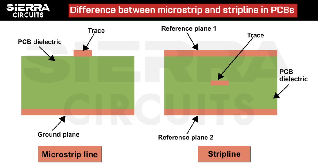
PCBs typically use two types of transmission lines: microstrips and striplines. Each of the transmission lines consists of a signal trace and reference planes.
The primary difference between microstrip and stripline configurations is the placement of the signal conductor. In a microstrip, the trace will be present on the outer layer of your circuit board. In stripline configurations, the conductor will be sandwiched between two reference planes.
Highlights:
- The dominant mode of propagation in microstrip is Quasi-TEM, leading to frequency-dependent phase velocity and characteristic impedance.
- Strategies to reduce microstrip losses include suspending the substrate over the air for reduced dielectric loss and wider traces for lower ohmic loss.
- Stripline, routed on internal PCB layers, provides shielding with signal traces between ground planes, reducing emissions and crosstalk.
- Stripline losses occur due to conductor conductivity, magnetic resonances, resistivity, and dielectric damping effects.
What are the differences between microstrip and stripline?
Microstrip traces run on the outer layer with one reference plane, while stripline traces are embedded between two planes. The latter offers better shielding and controlled impedance.
The infographic below summarizes the difference between these two geometries.

What is a microstrip line in a PCB?
The microstrip line is a planar transmission line that is used prominently in RF and microwave circuits. It is routed on the PCB surface and surrounded by two environments: PCB material and air.

A microstrip consists of a strip conductor (land) on a dielectric substrate backed by a ground plane that radiates when the spacing between the ground plane and the strip increases.
What is the mode of propagation in a microstrip line?
In microstrip, the dominant mode of propagation is Quasi-TEM (transverse electromagnetic). Due to this, the phase velocity, characteristic impedance, and field variation in the cross-section become frequency-dependent.

What is the effective dielectric constant (ϵeff) in a microstrip?
ϵeff for the signals on the microstrip will lie somewhere between that of the air and the dielectric. This is because the electric energy stored in the transmission line arrangement lies in the air as well as in the substrate. The effective dielectric constant determines the phase velocity of electromagnetic waves on the microstrip transmission line.
The microstrip line is dispersive. As frequency increases, the effective dielectric constant also increases towards the substrate, resulting in a decrease in phase velocity. The effective dielectric constant considers that most of the electric fields remain within the substrate, but a certain fraction of the total energy exists within the air above the board.

ϵeff also varies with the free-space wavelength. The dispersion becomes more significant with the decreasing ratio of strip width to substrate thickness/width/height. Dispersion is less prominent as the strip width increases. In that case, the microstrip appears to be an ideal parallel plate capacitor. ϵeff should be greater than the dielectric constant of air (ϵr = 1) and less than that of the dielectric constant of the substrate.
Read PCB Substrates: Knowing Your Dielectric Material’s Properties.

The problem related to microstrip parameter calculations is that the conductor strip is not immersed in a single dielectric material. On one side, it is dielectric, and on the other side, it is usually air.
The concept of effective dielectric constant is specially developed to address this challenge. The ϵeff represents some intermediate value between the relative dielectric constant of the board material (ϵr) and air (equivalent to 1). Hence, this can be used to compute microstrip parameters.
To learn more about board materials, download the PCB Material Design Guide.

PCB Material Design Guide
9 Chapters - 30 Pages - 40 Minute ReadWhat's Inside:
- Basic properties of the dielectric material to be considered
- Signal loss in PCB substrates
- Copper foil selection
- Key considerations for choosing PCB materials
Download Now
How to calculate the characteristic impedance of a microstrip line
The characteristic impedance of a microstrip line is calculated using an equation based on the laminate properties and trace geometry. Here’s the formula:

where,
- Z₀: characteristic impedance
- W: trace width
- T: trace thickness
- H: distance from the signal to the reference plane through the dielectric
- ϵr: relative permittivity (dielectric constant) of the PCB substrate
The characteristic impedance of the microstrip line changes with an increase in frequency. One point that is worth noticing here is that the IPC microstrip equation is most accurate between 50 and 100Ω, but is less accurate for lower/higher impedances.
Note: All dimensions are in mils.
The characteristic impedance of a transmission line can be expressed with distributed parameters:
Zo=√[(R+jωL)/(G+jωC)]
where,
- R: series resistance per unit length (Ω/m)
- L: series inductance (H/m)
- G: shunt conductance (mho/m)
- C: shunt capacitance (F/m)
An ideal, lossless transmission line has R = G = 0, and the characteristic impedance, Zo, reduces to √(L/C). Practically, the lines include losses that attenuate the signal. This signal attenuation is directly proportional to the trace length and the signal frequency.
Sierra Circuits fabricates and assembles PCBs with consistent impedance and a tolerance of ±5%. Visit our controlled impedance capabilities to learn more.
How to calculate the characteristic capacitance of a microstrip line
The characteristic capacitance of a microstrip line is calculated using an equation based on the substrate properties and trace geometry. Here’s the formula:

where,
- C₀: characteristic capacitance
- W: trace width
- T: board thickness
- H: separation between the traces
- ϵr: relative permittivity (dielectric constant) of the PCB substrate
What is the delay constant of a microstrip line?
For a given transmission line geometry, the delay constant is a function of the dielectric constant only and not the trace dimensions. With a given PCB laminate and dielectric constant, the propagation delay constant is fixed for various impedance lines. You can use the formula below to calculate it:

where,
- tpd: propagation delay
- Ereff: effective relative permittivity (dielectric constant) of the microstrip
To learn how to design low-loss trace geometries, download the PCB Transmission Line eBook.

PCB Transmission Line eBook
5 Chapters - 20 Pages - 25 Minute ReadWhat's Inside:
- What is a PCB transmission line
- Signal speed and propagation delay
- Critical length, controlled impedance and rise/fall time
- Analyzing a PCB transmission line
Download Now
What are the advantages of a microstrip structure?
A microstrip structure enables high-density routing with low crosstalk, faster signal propagation, and effective thermal and mechanical performance.
Below are the benefits:
- Microstrip is an ‘open’ line structure; it makes it very easy to connect components.
- It can be packed together with high density (multiple channels) with minimal crosstalk, making it suitable for RF and microwave IC design.
- Its planar topology is least affected by the PCB manufacturing process tolerances.
- It has a faster propagation time.
- This technique provides good heat sinking and mechanical support at the same time. Read 12 PCB Thermal Management Techniques to Reduce PCB Heating.
What are the sources of loss in a microstrip line?
Losses in a microstrip line arise from several physical mechanisms, such as finite conductivity and resistivity, radiation effects, and magnetic loss.
Here’s a quick overview of each of these loss sources.
- Finite conductivity of the line conductors results in conductor (ohmic) loss.
- Radiation effects are influenced by dielectric constant, substrate thickness, circuit geometry, and operating frequency.
- Magnetic loss becomes significant when magnetic substrates are used.
- Finite resistivity of the substrate leads to dielectric loss and damping effects.
Note: Despite microstrip’s low cost and compact size advantages, it is lossier than a coaxial line, waveguide, CPW, and stripline.
How to reduce losses in a microstrip line
It can be done by suspending the substrate in the air. Suspension of the microstrip means that the separation between the signal and ground paths increases, which also enhances the microstrip’s tendency to radiate, specifically at the discontinuities.

How suspension helps with loss reduction in a microstrip
The air between the bottom of the substrate and the ground plane contains the electromagnetic field. The insertion loss of the microstrip reduces because air essentially has no dielectric loss compared to standard circuit board substrates.
Additionally, the width of the microstrip line increases due to the lower effective dielectric constant. Wider lines have lower current density, and thus, lower ohmic loss. The microstrip suspension technique is used only up to a few GHz.
Note: A smaller width always leads to more losses.
What is a multi-layer microstrip line?
A multilayer microstrip line is a transmission line structure in which the signal trace is formed on one of multiple dielectric substrate layers, with one or more reference planes.
Microstrip geometry is used to conduct the EM waves at low frequency, but beyond 60GHz, its application is restricted due to the losses. This is the reason they cannot be used at THz frequencies.

With the need for SoC requirements, the use of multi-layered substrates has increased at a high frequency.
Advantages of multi-layered substrate material in microstrip construction
- Loss reduction and controlled coefficient of expansion
- Suitable for antenna design, where it provides sound surface wave immunity gain and bandwidth enhancement, along with good mechanical integration
Key takeaways
- Microstrip lines consist of a strip conductor on a dielectric substrate with a ground plane, widely used in RF and microwave circuits.
- Quasi-TEM mode is the dominant mode of propagation in microstrip, leading to frequency-dependent characteristics.
- Effective dielectric constant (ϵeff) determines phase velocity and varies with substrate properties, dimensions, and frequency, leading to dispersion effects.
- Various parameters like characteristic impedance, delay constant, and loss reduction techniques impact microstrip line design.
- Multi-layer microstrip configurations offer benefits like loss reduction, controlled expansion coefficients, and suitability for antenna design.
Talk to a PCB expert: Book a meeting or call us at +1 (800) 763-7503.
What is a stripline in a PCB?
A stripline is a transmission line structure routed on the inner layers of a PCB, where the signal trace is completely embedded within the dielectric material. It is typically used in multilayer boards, with the signal trace sandwiched between ground planes.

In a stripline, the current return path for a high-frequency signal trace is provided above and below the signal trace on the ground (power) planes. Due to this arrangement, the high-frequency signal remains inside the PCB, leading to fewer emissions and also providing shielding against incoming spurious signals.

A stripline transmission line consists of three layers of conductors, where the internal conductor is called the ‘sandwiched conductor’, while the other two, connected to the signal ground, are called the ground conductors. The sandwiched conductor is embedded in a homogeneous and isotropic dielectric, having a dielectric constant (Er).
The electric ‘E’ and the magnetic ‘H’ field lines for the fundamental TEM mode in stripline are indicated above in a defined cross-section and a defined time.
- The region between the outer conductors of the stripline contains only a single medium. That is the reason the phase velocity and the characteristic impedance of the fundamental mode (TEM) do not vary with frequency.
How to calculate the characteristic impedance of a stripline
The characteristic impedance of a stripline is determined by the dielectric constant of the substrate and the cross-sectional geometry of the center conductor and reference planes. The equation below is used to calculate the characteristic impedance of a stripline.

where,
- Z₀: characteristic impedance
- ϵr: relative permittivity (dielectric constant) of the substrate
- b: spacing between the two reference planes
- We: effective strip width of the center conductor
As the effective strip width (Wₑ) increases, the characteristic impedance of the stripline decreases.
Note: b is the spacing between two planes, and We is the effective strip width.
How to calculate the characteristic capacitance of a stripline
The characteristic capacitance of a stripline is calculated using an equation based on the PCB laminate properties and trace geometry. Here’s the formula:

where,
- C₀: characteristic capacitance of the stripline (pF/in)
- W: trace width
- T: trace thickness
- H: distance between the stripline and the reference plane through the dielectric
- ϵr: relative permittivity (dielectric constant) of the PCB substrate
What is the delay constant of a stripline?
The propagation delay for a given length in stripline is only a function of the dielectric. Here’s the formula to compute the delay constant of striplines:

where,
- tpd: propagation delay
- Ereff: effective relative permittivity (dielectric constant) of the microstrip

What are the advantages of a stripline arrangement?
A stripline arrangement offers improved signal integrity by providing superior shielding, lower electromagnetic emissions, and better EMI performance, especially at higher frequencies.
Here are the benefits:
- It provides shielding and protection to the signal traces.
- Low impedance, hence fewer emissions and crosstalk
- Improvement can be seen above 50MHz
- Stripline arrangement has better EMI characteristics.
Limitations of a stripline arrangement:
- Since stripline contains embedded signal traces, it is tough to debug such traces. In other words, PCB prototyping and troubleshooting would be difficult.
- Difficulty in decoupling
- Low impedance for proper matching
What are the losses in a stripline?
- Finite conductivity of its conductors
- Magnetic resonances
- Finite resistivity and dumping phenomenon of the dielectric
To learn about the root causes of signal attenuation and techniques to achieve uniform impedance in transmission lines, read our article, designing transmission lines with controlled impedance in high-speed PCB layouts.
Designing a multi-layer board with stripline geometry
Stripline is often required for multi-layer circuit boards because it can be routed between the layers, but grounding the stripline requires due attention. If the top and bottom ground planes are not at the same potential, a parallel-plate mode can propagate between them. If excited, this mode will not remain confined to the region near the strip but will be able to propagate wherever the two ground planes exist.
Stripline is less sensitive than microstrip to lateral ground planes of a metallic enclosure since the electromagnetic field is strongly contained near the center conductor and the top-bottom ground planes.
What will happen if the top and bottom ground planes are not at the same potential?
If the top and bottom ground planes are not maintained at the same potential, a parallel-plate mode can be excited between them. This mode is not confined to the region around the stripline trace; instead, it can propagate throughout any area where the two ground planes overlap. As a result, unwanted coupling, noise propagation, and signal integrity issues may occur.
The parallel-plate mode can be suppressed by:
- Using metalized via holes connecting the top and bottom ground planes
- Placing vias closely (spacing between vias should be 1/8 of a wavelength in the dielectric to prevent the potential difference between the ground planes).

If vias are placed too close to the stripline edge, they may interfere with the characteristic impedance. So, the via spacing should be a minimum of three strip widths.
So, is it possible to design a multi-layer PCB without using a stripline arrangement?
The embedded trace can be replaced by a double two-layer PCB design, i.e., four copper layers in total.

The traces routed at the top PCB surface form a microstrip with the power plane, while the bottom traces form a microstrip with the ground plane.
Here, the signal traces of both outer layers are easily accessible for measurement and board troubleshooting purposes. However, this arrangement does not take advantage of the shielding properties of the planes, leading to greater emissions and sensitivity towards external signals.
The arrangement given on the right side of the above image uses the embedded traces and takes full advantage of the planes. The choice between embedded and non-embedded arrangements for PCB designing can be made selectively based on what is important for you. Ease of testing or reduced EMI and EMC.
Key takeaways:
- Stripline configurations offer excellent shielding, low emissions, and improved EMI characteristics.
- Proper grounding techniques, including metalized via holes and careful via spacing, are essential to suppress parallel-plate modes and maintain signal integrity.
- Designers can opt for alternative configurations like embedded traces in double two-layer PCBs, balancing testing ease and EMI considerations.
7 routing techniques using microstrip and stripline
Apart from manufacturing and dielectric differences, PCB microstrip and stripline designs have routing differences as well.
- Microstrip routing: Transmission lines that are routed on the external layers are considered to be microstrip. Their modeling depends on the trace thickness and width, and the substrate height and dielectric type.

- Microstrip differential pair routing: This technique is used for routing differential pairs and has the same arrangement as regular microstrip routing, but its model is more complex due to the additional trace spacing for the differential pair.

- Embedded microstrip routing: This structure is similar to a regular microstrip except that there is another dielectric layer above the transmission line.

- Coplanar microstrip routing: In coplanar microstrip routing, the signal trace is routed in parallel to two ground planes. These ground planes provide natural shielding for the signal against interference from other traces on a board.

- Stripline routing: In this technique, the traces are routed on internal layers. Like microstrip, its modeling is based on the trace thickness and width, the substrate height, the dielectric type, and the calculations for the trace being embedded between the two planes.

- Coplanar stripline routing: In coplanar stripline routing, the signal trace is internally routed in parallel to two ground planes.

- Broadside-coupled stripline routing: This technique is also used for routing internal layer differential pairs.

What is the impact of surface finish and copper roughness on conductor loss?
Surface finish and copper roughness directly affect conductor loss by altering current distribution at high frequencies. Lower-conductivity finishes and increased surface roughness lead to higher insertion loss and degraded signal performance.
The detailed effects are summarized below:
- Surface finish impacts the conductor loss due to high current density at the edge of the conductor.
- Most metal finishes used in the PCB industry are less conductive than copper (gold, nickel, aluminum, brass, solder, tin). Lower conductivity causes higher conductor losses, which increases insertion loss. Silver is the exception and does not increase copper conductor loss.
- The gold finish is very thin (about 0.05um), but skin depth will not approach this thickness until the frequency is about 1THz.
- Electroless Nickel Immersion Gold (ENIG) finish is widely used since it protects the Nickel from oxidation.
- When skin depth is close to the dimension of copper surface roughness or less, the surface roughness will significantly increase the conductor loss, which ultimately slows down the wave propagation.
- Some degree of copper roughness is always applied to promote adhesion to the dielectric material and improve the peel strength of the laminate.
- The electrical impact of conductor roughness increases with frequency, increases the capacitance, increases the group delay, decreases the characteristic impedance over a wide bandwidth, and apparently increases Dk to match the group delay vs. frequency characteristic.
- Ohmic and dielectric losses in a microstrip limit its power handling capacity.
- An increase in temperature due to conductor and dielectric losses limits the average power of the microstrip line. In contrast, the breakdown between the strip conductor and ground plane limits the peak power.
Dielectric constant and guided wavelength of microstrip and stripline designs
Dielectric constant (how electrically dense the material is to vacuum) and loss tangent (how lossy the material is) are two critical parameters required for application-specific PCB trace design.
The dielectric constant of the PCB material is greater than 1. It lies between the dielectric constants of vacuum and air. Thus, the guided wavelength on the PCB will be shorter than the wavelength in vacuum/air, and the propagation velocity will also be lower than the speed of light.
If the dielectric constant is higher, then the guided wavelength will be shorter. That is why the same length mismatch between two traces causes more propagation delay. Considering this fact, it is advisable to use a material with a low dielectric constant.

For stripline, the guided wavelength is:

where,
- λg: guided wavelength in the stripline
- c: speed of light in free space
- f: operating frequency
- ϵr: relative permittivity of the substrate
For microstrip, the guided wavelength is:

where,
- λg: guided wavelength in the microstrip line
- c: speed of light in free space
- f: operating frequency
- ϵeff: effective relative permittivity of the microstrip
ϵeff depends on the trace width (w), height between the signal trace and ground plane (h), and ϵr.
For the same material, the signals will propagate faster in the microstrip than in the stripline.

It is quite important to accurately design stripline and microstrip transmission lines to achieve appropriate impedance matching and/or pulse delay time. Understanding the fundamentals of microstrip and stripline routing helps PCB designers in applying these indigenous circuit technologies to their designs.
In a microstrip configuration, the guided wavelength is determined by dividing the free space wavelength (which corresponds to the wavelength of light) by the square root of the effective dielectric constant (ϵeff). This dielectric constant depends on factors such as trace width (w), the distance between the signal trace and ground plane (h), and the relative permittivity (ϵr). For identical materials, signals travel faster in microstrip compared to striplines due to these factors.
Two primary transmission line configurations, microstrips and striplines, have distinct characteristics and applications in RF and microwave circuits. These transmission lines consist of signal traces and reference planes, with specific electromagnetic field distributions. Routing techniques like microstrip, coplanar microstrip, stripline, coplanar stripline, and broadside-coupled stripline cater to diverse design requirements.
Understanding these fundamentals is essential to creating optimized microstrip and striplines and ensuring appropriate impedance matching and signal delay in your designs.
Have queries regarding microstrip and striplines? Post them on our forum, SierraConnect. Our design experts will resolve them.