Contents

On-demand webinar
How Good is My Shield? An Introduction to Transfer Impedance and Shielding Effectiveness
by Karen Burnham
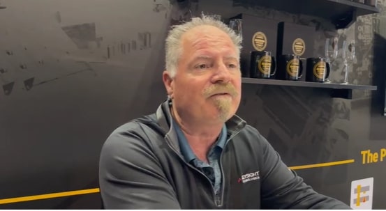
We got an opportunity to talk to Mike Resso of Keysight during DesignCon 2022 . Watch the video to find out all about it.
Mike Resso is a signal integrity application scientist and works for the Internet Infrastructure Group of Keysight Technologies. He has an experience of over 30 years of in the test and measurement industry. His most recent activity has focused on the complete multiport characterization of high-speed digital interconnects using TDR and VNA.
What are the challenges involved in designing and testing channels at 224 Gbps?
Mike: The new, faster data rates are typically a PAM-4 modulation (pulse amplitude modulation-4). Instead of just measuring one eye diagram to see the performance of the channel, you have to measure three eyes. And subsequently, there are going to be different rise times and fall times, and jitters in PCBs that need to be added to the normally heavy load of the tested measurement techniques for compliance and validation.
Can you tell us what the limiting factors are due to copper interconnects?
Mike: Most of the signal integrity challenges will be reflections from impedance discontinuities. There will be insertion loss from perhaps lossy dielectric material. It is all zeros and ones. And as you transition from a 0 level to a 1 level 1, the faster the rise time, the more reflections become a problem. You have to mitigate that by doing reactive compensation. You may have to add some inductance to a via or subtract a little bit of capacitance in a transmission line. These are just things on PCB layout that need to be looked at and analyzed carefully.
What is the significance of S-parameter analysis in modern simulation?
Mike: This is the design cycle that before you build something, you simulate it to predict what the performance will be. This gives you a very good idea of what problems will pop up once you build a prototype. S parameters (scattering parameters), give you a way to accurately characterize the transmission and reflection properties that can be used in simulation programs to give you an understanding of performance levels. Then once you have your prototype built, you can do real measurements compared to the simulations and then refine all of your models. Going forward, when you know, the data rates will increase even further, you have that experience from the simulation and the measurement correlation to move to even faster speeds, which are inevitable for today’s internet infrastructure.
Signal Integrity eBook
6 Chapters - 53 Pages - 60 Minute ReadWhat's Inside:
- Impedance discontinuities
- Crosstalk
- Reflections, ringing, overshoot and undershoot
- Via stubs
Download Now
How do you determine the appropriate time-domain measurement instrument: TDR or VNA?
Mike: TDR, time domain reflectometer is an oscilloscope-based measurement technique. If you are a high-speed digital engineer, that is typically your instrument of choice. If you happen to be a microwave engineer, where you have high-frequency domain information in your education, you tend to look toward the vector network analyzer, VNA, to make the same measurements. Basically, you can take the results from either one and either do a fast Fourier transform or inverse fast Fourier transform to get the same data in either domain. The bottom line is the vector network analyzer will give you a better dynamic range. So ultimately if you have a choice and you are familiar with both, you most likely will choose the VNA.
High-Speed PCB Design Guide
8 Chapters - 115 Pages - 150 Minute ReadWhat's Inside:
- Explanations of signal integrity issues
- Understanding transmission lines and controlled impedance
- Selection process of high-speed PCB materials
- High-speed layout guidelines
Download Now
How do you select the right one according to the application?
Mike: You can look at it in either domain. But in particular, if you have a high crosstalk environment, you need to pull a small signal out of the noise. That can only be accomplished with an instrument that has a high dynamic range, that is the VNA, because it has a very narrow half-power bandwidth on the receiver. You can look at very low noise floors and you will be able to spot that crosstalk. Otherwise, if you use a broad bandwidth instrument, perhaps like the TDR, the crosstalk is going to be buried in the noise and you just will not see it.
Do you find any uncertainty in the measurement of TDR and VNA? If so, what influences that uncertainty?
Mike: All instruments have uncertainty. Some of them are systematic, and some are due to the environment. The calibration techniques of the vector network analyzer are always a bit more sophisticated because of the high-frequency content that needs to be accurate. You can have a short, open load through calibration that will give the most accurate information at the reference plane. TDR calibration is still there but is not as versatile as the VNA. It is a great tool for getting an intuitive feeling of what is going on in a circuit or interconnect, but ultimately if accuracy is the main component, the VNA is usually the instrument of choice.
What are the benefits of VNA?
Mike: The main advantages are high dynamic range and sophisticated calibration techniques. You can have a scalable VNA, like the PXI VNA that can be easily configured anywhere from 2 ports up to 32 ports. This gives you incredible flexibility, both in manufacturing and the R&D lab. If you have six differential channels on one motherboard, that is 12 input and 12 output, it is a 24-part measurement. You could do that with one single instrument with a scalable VNA.
How significant is it to use time and frequency domain analyses for simulation and measurements on a given channel design?
Mike: I found both domains, time and frequency are invaluable. The reason is when you converse, you can be versatile enough in both domains, it is like speaking in two languages. You can look at time-domain data to get the impedance profile and identify not only how much excess capacitance you have in a via, but also where that via is located spatially within the channel. Then you can switch to the frequency domain and can look at insertion loss, and see what frequencies are being attenuated due to that via capacitance. So, using these two domains in parallel gives you a whole different insight into optimizing your design for high speed.

Do you know any tools to identify and resolve the root causes of signal integrity problems?
Mike: The vector network analyzer has a very large portfolio of benchtop, portable, scalable, and frequency ranges from 9 GHz up to 120 GHz. The most helpful tool that I found for high-speed digital engineers is an application for signal integrity called physical layer test system software. This is built for digital design engineers. It will allow them to make a VNA do backflips without really having to be a frequency domain expert.
How do you describe MOI using the Keysight vector network analyzer? What are its capabilities?
Mike: MOI stands for a method of implementation. It is a recipe book for how to make a particular measurement for any application. MOI is typically a word document that has pictures and step-by-step instructions for how and which buttons to be pressed so that if you have a technician, he also can run through a very sophisticated measurement if he follows MOI word by word. This is typically a different protocol used for devices under test.
About Poulomi Ghosh : Poulomi is a microwave engineer specializing in EMI, EMC, RF, and high-speed electronics. As a senior technical writer at Sierra Circuits, she creates advanced engineering articles and webinars for hardware engineers and PCB designers.


