



Contents

On-demand webinar
How Good is My Shield? An Introduction to Transfer Impedance and Shielding Effectiveness
by Karen Burnham
Semi-additive process (SAP) and modified semi-additive process (mSAP) are advanced PCB manufacturing technologies that build conductive features additively rather than etching them from copper foil.
These processes support finer line widths, tighter spacing, improved impedance control, and higher routing densities than conventional subtractive etching.
SAP supports the finest features required for advanced packages. mSAP provides a more economical solution for high-volume applications such as smartphones and substrate-like PCBs (SLPs).
Layout engineers designing ultra-high-density interconnect (UHDI), high-speed, RF, or SLP boards should understand the differences between additive technologies to choose the most suitable process for their application.
In this article, you’ll learn about SAP and mSAP workflows, how they differ from conventional subtractive etching, and design strategies that help you improve yield.
Highlights:
- Choose SAP for trace geometries below 15 microns and SLPs where maximum routing density is necessary.
- Use mSAP when you need fine-pitch routing with better manufacturability and lower cost.
- Clearly define additive layers in the stack-up to avoid miscommunication.
- Do not combine additive and subtractive processes on the same layer, as it introduces yield and process-control issues.
Why SAP and mSAP for ultra-fine PCB features
As trace widths continue to shrink in advanced printed boards, traditional etching struggles to maintain dimensional accuracy and yield. Additive copper build-up improves trace geometry control and enables ultra-fine routing for modern electronic systems.
Traditional subtractive etching cannot achieve this as it removes copper from relatively thick foil, making it difficult to maintain precise trace widths, spacing, and impedance at very small geometries.
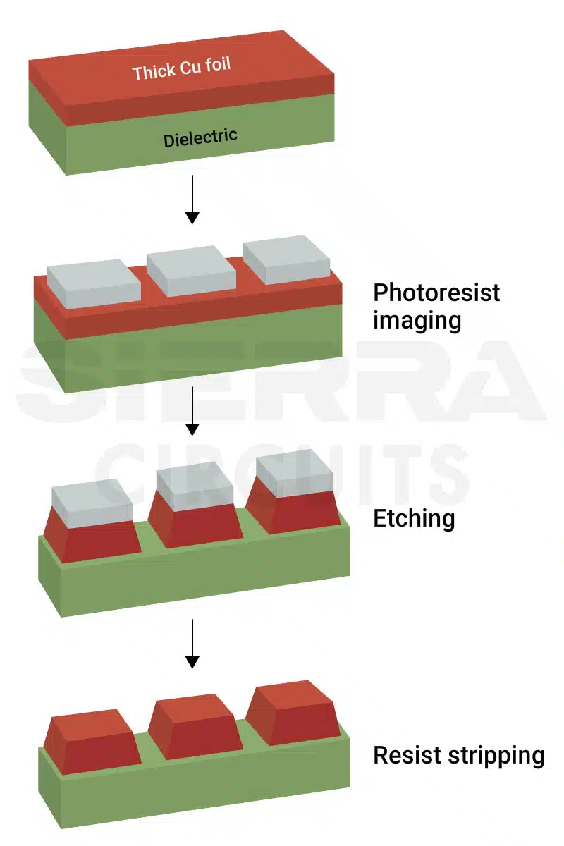
The conventional subtractive process starts with a copper-clad laminate in which a copper foil covers the entire surface, typically 1/2 oz to 1 oz or higher.
A photoresist pattern is applied to protect the desired circuit traces, and the unwanted copper is then chemically etched away to form the circuitry.
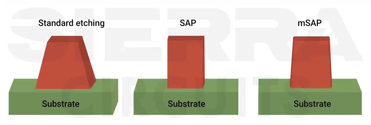
Since the process removes copper from thick foil, the copper etching occurs both vertically and laterally, resulting in undercutting and trapezoidal trace profiles with narrow tops and wider bottoms.
This approach runs into several issues:
- Etch undercut: Etchant attacks copper laterally as well as vertically, making it hard to maintain accurate line width at very small scales.

An illustration of etching undercut on a PCB trace. Non-vertical sidewalls: Traces take on a trapezoidal cross-section, affecting impedance and signal integrity.
- Reduced yield: At very low line/space (e.g., < 50 microns or < 2 mil), maintaining yield and consistency becomes increasingly difficult.
- Copper loss and rough surface: More etching means higher roughness and more variation, which can increase loss at high frequencies.
This process remains cost-effective and reliable for conventional PCB designs. Its geometric limitations, higher conductor loss, and reduced dimensional precision make it less suitable for UHDI, advanced packaging, and SLP technologies.
To support smartphones, 5G modules, advanced wearables, and high-density interposers, manufacturers need processes that build copper only where needed with tight dimensional control, and this is exactly what SAP and mSAP PCB manufacturing processes provide.
For more on ultra-HDI circuit boards, download the UHDI PCB Design and Manufacturing guide.

UHDI PCB Design and Manufacturing
8 Chapters - 65 Pages - 62 Minute ReadWhat's Inside:
- UHDI characteristics and fabrication technologies
- Material and stack-up considerations
- DFM guidelines for ultra-HDI PCBs
- Causes of yield loss in 2/2 mil fabrication
Download Now
What is SAP technology in circuit board manufacturing?
SAP is a circuit board manufacturing method that creates ultra-fine copper features by electroplating copper where needed, rather than etching traces from copper foil.
Depending on the manufacturing process and fabricator capability, the semi-additive process can support line/space geometries less than 15 microns (0.6 mil) wide, making it suitable for IC substrates, advanced packaging, and other high-density applications.
Since copper is deposited only at the desired location, SAP minimizes the amount of copper removed during manufacturing. This significantly reduces undercutting and allows tighter control of conductor dimensions than conventional subtractive etching
| Parameters | Specifications |
|---|---|
| Seed layer thickness | ~0.1 – 0.5 µm (~0.004 – 0.02 mil) |
| Line/space capability | ~5 – 15 µm (~0.2 – 0.6 mil) |
| Copper thickness after plating | Typically, ≤10 µm (≤0.4 mil) |
| Process requirements | Sputtering and tight process control |
| Benefits | Precise control over dielectric thickness, trace cross-section, and layer-to-layer registration |
How does the semi-additive process work?
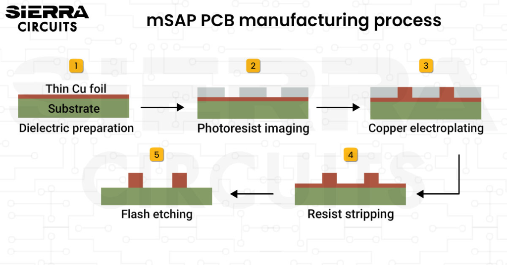
The process begins with depositing a very thin copper seed layer on the dielectric surface.
Next, photoresist is patterned to define the circuitry, and copper is electroplated in the exposed areas.
After plating, the remaining exposed seed layer is lightly etched away (flash etch), leaving behind highly defined copper features with straight sidewalls and minimal undercutting.
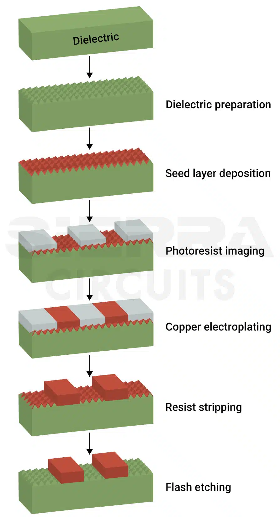
- Dielectric preparation: The process begins with a bare dielectric. The surface is chemically treated or roughened (often via a permanganate desmear or plasma treatment) to create micro-voids for mechanical bonding of the seed layer.
- Seed layer deposition: An ultra-thin conductive seed layer of sputtered copper (typically ~ 0.5 microns) is deposited across the entire circuit board panel, making the non-conductive surface receptive to electrolytic plating.
- Photoresist imaging: A dry film or liquid photoresist is applied, exposed, and developed. The resist is removed from the areas where the traces and pads should be formed.
- Copper electroplating: Electrolytic copper is plated into the open channels of the photoresist, building the trace to its full required thickness.
- Resist stripping: The photoresist is stripped away, leaving the plated copper traces sitting on top of the thin, continuous seed layer.
- Flash etching: This step removes the exposed seed layer between the traces. Since the seed is so thin (almost zero), this step completes in seconds, leaving the main traces intact with vertical sidewalls.
During flash etching, only an ultra-thin seed layer is stripped away, so the plated copper features remain nearly the same. This is one of the main reasons SAP reliably achieves extremely fine traces and spaces.
The board now primarily contains additively plated copper instead of leftover thick foil. This method is called semi‑additive because there is typically some initial thin conductive layer (seed) and a minor etch step.


What is mSAP technology in PCB manufacturing?
mSAP is a modified version of the semi-additive process optimized for high-volume production.
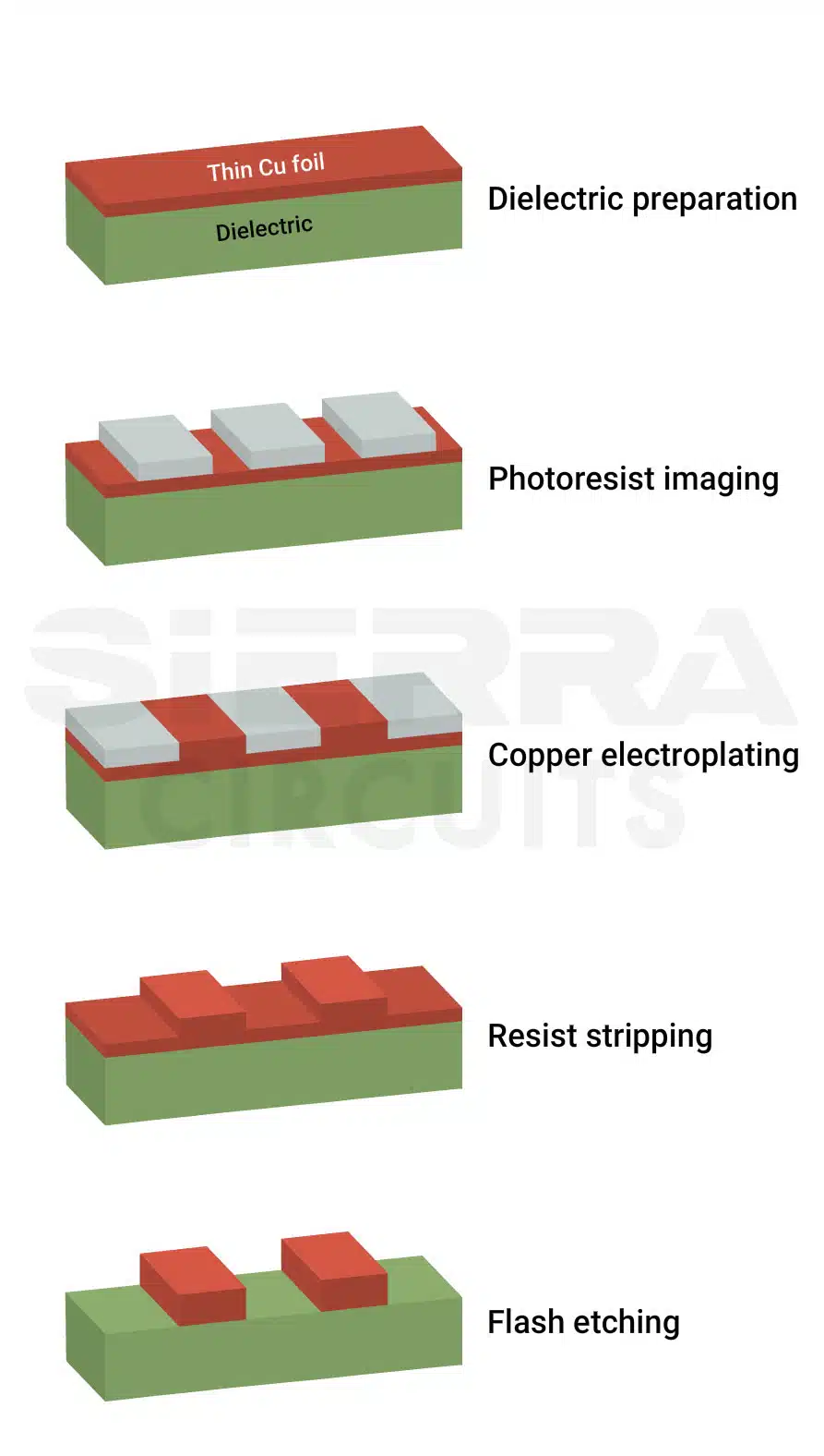
This process selectively adds electrolytic copper to a thin laminated copper foil (typically ~1.5 microns) on a dielectric substrate, and then flash-etches the exposed foil between traces.
As a result, mSAP offers a lower-cost alternative to full SAP while still enabling finer pitches than traditional subtractive etching.
| Parameters | Specifications |
|---|---|
| Seed layer thickness | ~1.5 – 5 µm (~0.06 – 0.2 mil) laminated copper foil |
| Line/space capability | ~15 – 40 µm (~0.6 – 1.6 mil) |
| Copper thickness after plating | Typically ≤10 – 18 µm (≤0.4 – 0.7 mil) |
| Process requirements | Standard HDI fabrication lines with moderate upgrades for plating and etching control |
| Benefits | Enables fine-pitch routing at lower cost and higher production scalability than SAP |
mSAP is particularly well suited to high-density PCB designs where conventional subtractive etching cannot reliably maintain fine line widths and spacing. Its ability to use ultra-thin copper foil and controlled additive plating makes it a practical manufacturing approach for ultra-HDI applications.
How does the modified semi-additive process work?
The mSAP workflow resembles SAP but starts with a thin copper foil instead of a deposited seed layer.
mSAP is a primarily additive copper patterning method used for fine features. Its workflow resembles SAP but starts with a thin copper foil.
Here are the steps:
- Dielectric preparation: The process begins with a thin copper-clad laminate. Fabricators lightly treat or etch the surface to optimize adhesion and reduce foil thickness if necessary.
- A thin laminated copper foil (typically ~1.5 microns) serves as the conductive base across the panel; no separate electroless deposition is necessary. In some cases, a standard foil is pre-reduced through a uniform micro-etch to reach the desired seed thickness.
- Photoresist imaging: A dry film or liquid photoresist is applied, exposed, and developed. The resist is removed from the areas where the traces and pads should be formed, exposing the base foil for plating.
- Copper electroplating: Electrolytic copper is plated onto the exposed foil areas, building the trace to its full required thickness.
- Resist stripping: A chemical stripping agent removes the photoresist, leaving the plated copper traces on top of the continuous thin foil layer.
- Flash etching: A brief, differential etch removes the exposed base foil between the traces.
Additively plated copper makes up the majority of copper on the board, with the initial foil acting as a modified seed.
According to Sridhar Kasichainula, Head of Technology at Sierra Circuits, “Copper foil roughness still matters in mSAP PCB manufacturing because the process starts with an extremely thin copper foil, typically around 1.5 microns, as the seed layer. Although most of the final copper is built up through plating, the starting copper surface influences copper deposition, adhesion, and the final copper topology. Therefore, the additive nature of mSAP does not eliminate the need to control the starting copper surface.”
The key advantage of the thin base foil becomes apparent during the flash-etch step. During etching, copper is removed not only vertically but also laterally beneath the trace edges. With a conventional ~18 microns copper layer, a greater amount of copper must be etched away, increasing lateral etching and potentially reducing the final trace width. In mSAP, the initial foil may be only ~1.5 microns thick, so the amount of base copper that must be removed during flash etching is much smaller. This significantly
reduces lateral etching and helps produce straighter trace sidewalls and more consistent fine features.
mSAP should not be viewed as a standalone solution for UHDI fabrication. It is one part of the overall UHDI build process, working together with material selection, dielectric thickness, laser drilling, via formation, plating, imaging, registration control, and other process controls required to achieve the desired fine-feature performance. This technology makes producing fine lines easier by reducing etching-related limitations. The overall UHDI capability depends on controlling the complete manufacturing process.
Sierra Circuits utilizes self-learning automated scaling software (XACT) to ensure precision in HDI stack-up design. The system analyzes material type, thickness, and copper weight on each layer to accurately predict and compensate for material shrinkage.
Our engineers optimize your stack-up, materials, and design for manufacturability to support demanding 2/2 mil UHDI designs.
Visit UHDI PCB capabilities to learn more.
Can you combine additive and subtractive processes on the same circuit board layer?
Combining additive and subtractive processes on the same circuit board layer is not practical because the two processes require different starting copper thicknesses, imaging accuracy, plating sequences, and etching conditions. Trying to support both on the same layer adds process complexity, narrows the manufacturing window, and can reduce yield.
Key challenges include:
- Different copper thickness requirements: Additive processes use an ultra-thin seed layer or copper foil, whereas subtractive processing starts with thicker copper foil. Supporting both on the same layer complicates fabrication.
- Varied etching requirements: Subtractive processing removes thick copper, whereas SAP and mSAP PCBs use a controlled flash etch to remove only the thin seed layer. A single etching process cannot optimize both.
- Tighter imaging requirements: Ultra-fine features require tighter imaging and registration control than conventional routing. Supporting both feature sizes on one layer narrows the manufacturing process window.
- Greater process complexity: Imaging, plating, stripping, and etching must be controlled within much tighter tolerances, making it harder to maintain consistent line widths, spacing, and registration.
- Lower manufacturing yield: Small variations in plating, etching, or registration have a greater impact on fine features, increasing the risk of defects and reducing yield.
Why combining additive and subtractive processes doesn’t work
Additive and subtractive fabrication methods rely on different assumptions for starting copper thickness, plating sequence, imaging accuracy, and etch behavior.
In subtractive manufacturing, the circuit pattern is formed by selectively protecting the desired copper and etching away the unwanted copper. In the additive process, copper is built up in the required circuit areas, and the remaining seed layer or thin copper foil is subsequently removed.
Recommended approach
Instead of combining manufacturing methods on the same layer, assign them to different layers. Use mSAP for high-density signal layers and conventional subtractive processing for power, ground, or standard routing layers. This approach allows each layer to be manufactured using the process best suited to its feature requirements.
Subtractive vs. SAP vs. mSAP PCB manufacturing technologies
The three processes differ primarily in how copper is introduced and removed during circuit formation. Subtractive manufacturing starts with relatively thick copper and removes unwanted material. SAP starts with an ultra-thin conductive seed layer and builds the circuit through plating. mSAP starts with thin copper foil and similarly builds most of the final conductor thickness through additive plating
| Feature | Subtractive | SAP | mSAP |
|---|---|---|---|
| Process | Starts with thick copper and removes unwanted copper through etching | Starts with an ultra-thin deposited seed layer and builds copper features through electroplating | Begins with ultra-thin copper and forms the desired copper through electroplating |
| Start copper thickness | 12 – 35 µm
(~0.47–1.38 mil) |
Seed layer or near-zero copper | Ultra-thin foil (e.g., 1 – 5 µm (~0.04 – 0.2 mil)) |
| Circuit formation | Etch defined | Additive plating + light etch | Additive plating + light etch |
| Typical line/space capability | >50 µm and above (2 mil+) | ~5 – 15 µm (~0.2 – 0.6 mil) in advanced substrates | ~15 – 40 µm (~0.6 – 1.6 mil) depending on fab capability |
| Sidewall profile | Trapezoidal, significant undercut | Almost vertical | More vertical, reduced undercut |
| Cost and complexity | Lowest | Highest | Medium |
| Applications | Standard multilayer/HDI | UHDI (flex/rigid), IC substrates | Ultra-HDI, SLPs, and high-speed/RF |
In practice, the manufacturing process is often selected based on the minimum line/space requirement, production volume, and budget. Conventional subtractive processing remains the preferred choice for standard multilayer PCBs; mSAP can support fine geometries used in ultra-HDI circuit board designs, and SAP is primarily reserved for the finest IC substrates and advanced package applications.
What are the challenges in additive PCB fabrication?
SAP and mSAP boards are more difficult to manufacture because they rely on ultra-thin copper layers, fine-line imaging, precise plating control, tight registration, and specialized materials. At 2-mil-and-below geometries, small variations in imaging, resist formation, plating, etching, or material movement can significantly affect the final trace dimensions and spacing.
Furthermore, additive processes shift much of the dimensional control from etching to imaging, resist formation, and copper plating. Designers should therefore work with the fabricator to establish a realistic process window for the required line/space, copper thickness, registration, and microvia structures rather than relying only on published minimum feature sizes.
1. Maintaining seed-layer uniformity across the panel
The starting conductive layer must remain sufficiently uniform across the panel (±10% thickness variation) to support consistent electroplating and fine-line formation.
Thin spots (<0.3 microns) can cause open circuits after etching, while thick spots (>1.2 microns) risk shorting between fine-pitch traces.
Fabricators employ advanced deposition systems and monitor chemistry (e.g., pH, copper concentration) to maintain uniformity.
For SAP and mSAP designs, seed-layer uniformity is particularly important because fine-line structures leave little room for dimensional variation. Nonuniform seed-layer thickness can affect plating behavior, final conductor dimensions, and flash-etch performance. Designers should therefore confirm the fabricator’s qualified seed-layer process when working with very fine geometries.
2. Imaging errors at 2-mil-and-below geometries
Imaging transfers the circuit pattern from the artwork or phototool onto the photoresist. At 2-mil and below, the features are so small that exposure, alignment, resolution, and resist uniformity become critical. The smaller the feature, the less process margin you have for imaging errors.
The photoresist pattern defines the precise openings where copper is plated, so exposure, optical alignment, focus, resist thickness, and development must be controlled together. Achieving reliable sub-2 mil features requires high-resolution direct imaging (LDI) systems and fine-line photoresists capable of resolving these extreme geometries.
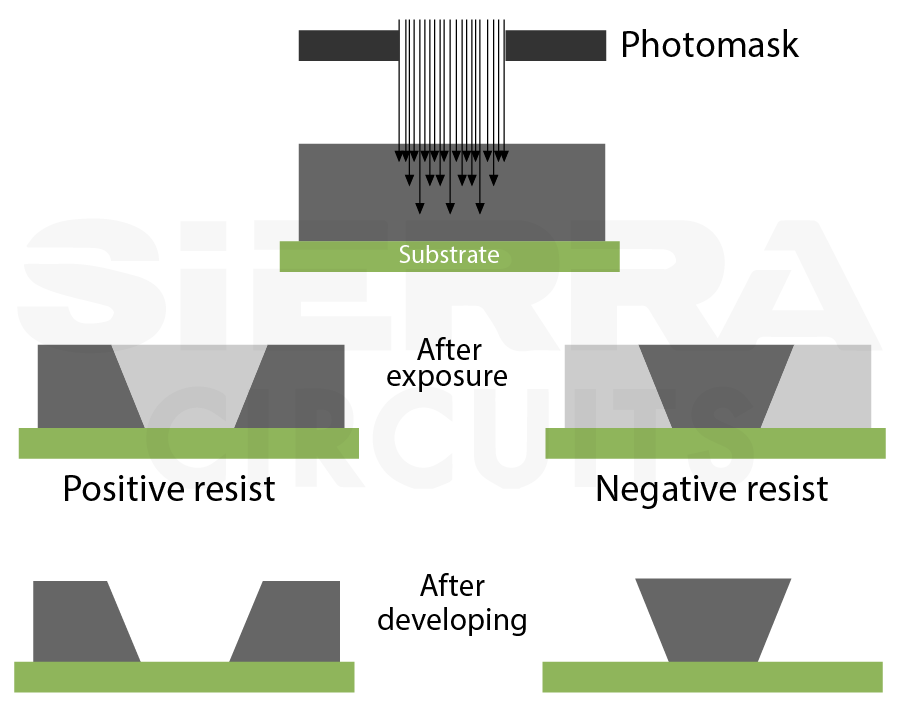
Follow the practices below to achieve better imaging:
- Define line/space requirements based on the fabricator’s qualified imaging capability.
- Account for layer-to-layer registration and dimensional movement when placing fine features.
- Avoid unnecessarily long runs of ultra-fine traces when wider geometry can meet the electrical requirements.
- Confirm the fabricator’s achievable finished line width and spacing rather than designing to the theoretical imaging resolution.
At Sierra Circuits, our manufacturing experts maintain tight control of exposure energy, focus, alignment, and resist uniformity across the panel.
We optimize development conditions so the intended resist pattern is consistently formed. This will minimize image distortion and linewidth variation caused by exposure, resist thickness, and process conditions.
3. Matching resist thickness to trace height
In mSAP, the copper seed layer is very thin, so most of the finished trace thickness is built up by electroplating inside the openings in the photoresist. The photoresist essentially acts as a mold that defines the width and shape of each trace.
As the plated copper gets taller, it can also grow sideways near the top of the trace. This lateral growth can reduce the spacing between adjacent traces and affect the final line/space geometry. For this reason, the photoresist thickness, trace geometry, and finished copper thickness must be considered together.
- Choose the right resist thickness for fine features: Finer line/space geometries require a high-resolution photoresist. In general, thinner resist provides better resolution. A photoresist thickness of about 15 microns is considered optimal for fine resolution, while 30 microns is about the practical maximum. Using a resist that is thicker than necessary can make it more difficult to maintain very fine features.
- Sierra Circuits uses high-resolution photoresists selected according to the required line/space and finished copper thickness. Thinner photoresists can support finer features, but the final resist thickness is determined by the fabrication process and design requirements.
- Keep plated copper well below the resist height: Because most of the conductor thickness is plated into the resist openings, the finished copper thickness should be kept as low as practical and well below the resist thickness. This provides sufficient margin during plating and helps prevent copper from growing sideways over the resist edges.
- Avoid over-plating: Over-plating can cause the copper to mushroom over the edges of the resist, reducing the intended spacing between adjacent traces. Once this happens, the feature geometry cannot be recovered through rework. Fabricators therefore need to maintain sufficient margin between the target finished copper thickness and the resist height and tightly control the plating process.
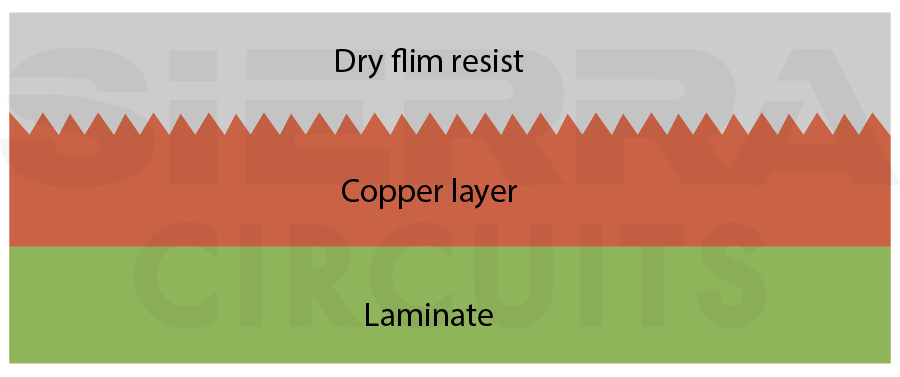
For UHDI layouts, specify the finished copper thickness together with the target line/space geometry, photoresist thickness, and plating tolerances rather than treating these parameters independently. Keeping the plated copper as thin as the design allows, while maintaining adequate resist height, gives the fabricator more process margin for producing consistent fine-line features.
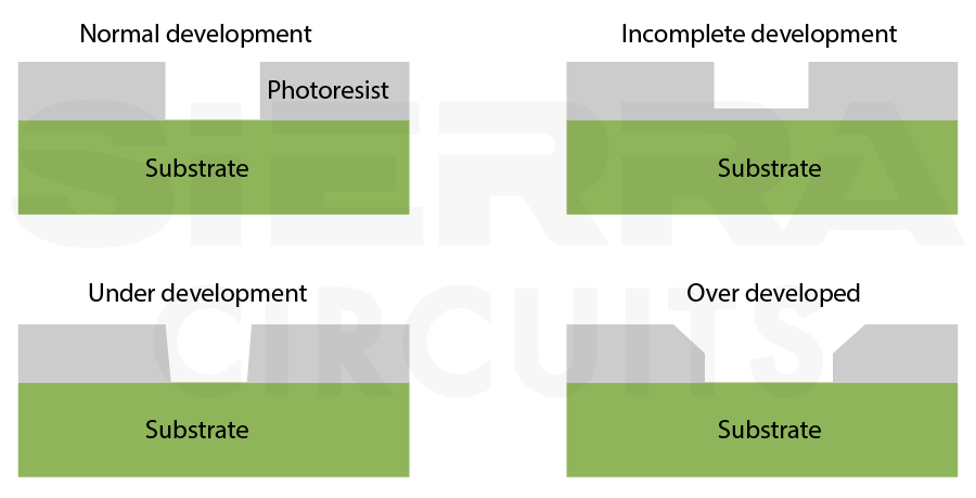
4. Controlling the resist profile during imaging and development
The developed resist opening must accurately reproduce the intended circuit pattern because the opening determines where copper is deposited during pattern plating.
The resist profile is affected by:
- Exposure dose
- Focus and imaging conditions
- Resist thickness
- Development chemistry and time
- Resist uniformity
- Copper surface condition
A well-controlled resist profile provides a clearly defined plating opening and helps maintain the intended trace width and spacing. Poor profile control can distort the opening and contribute to variation in finished conductor dimensions.
At 2-mil-and-below geometries, even small changes in the resist opening can significantly affect the finished conductor dimensions. As a PCB designer, you should:
- Account for the finished trace dimensions rather than relying only on nominal resist-opening dimensions.
- Avoid unnecessarily aggressive line/space combinations when the electrical requirement can be achieved with more manufacturable geometry.
5. Understanding current-density distribution during plating
Electrolytic copper plating does not deposit uniformly across every feature on a panel. Current density varies with feature geometry, feature density, surrounding copper, and panel location. High-current-density regions can receive more copper, while isolated or shielded features can receive less.
This becomes particularly important for additive designs because a single isolated 2-mil trace can behave differently from traces located within a dense routing field.
Where practical:
- Avoid isolated fine-line features when the electrical design allows them to be grouped with surrounding copper.
- Maintain balanced copper distribution across the panel.
- Copper thieving or dummy patterns can help balance current distribution across the panel.
- Review isolated traces located away from dense copper regions with the fabricator.
- Confirm that the fabricator can achieve the required finished copper thickness on both dense and isolated features.
- Ask your fabricator to measure finished line width and spacing to verify that the plated geometry remains within specification.
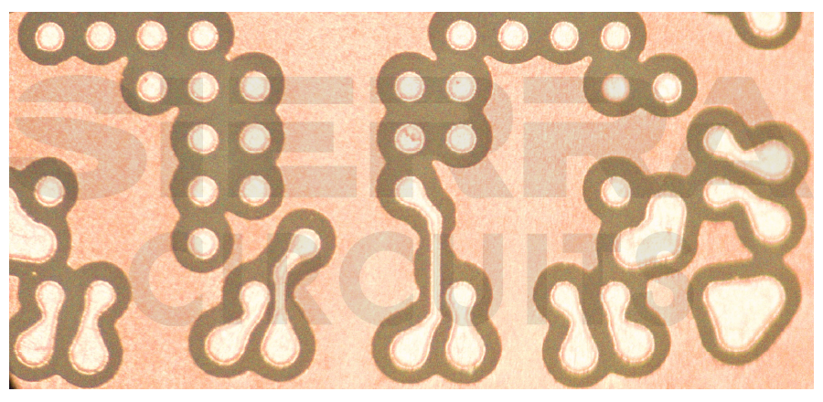
These are 1-mil lines and 3-mil pads within a plane area. The high-density plane area will draw most of the plating current. Hence, the small internal features, which are at lower current density, will get less current.
6. Plating inaccuracy around microvias and fine-line structures
Additive plating must produce reliable copper deposition in both laser-drilled microvias and narrow fine-line openings. Microvias require consistent copper deposition and filling, whereas fine-line structures require control of copper thickness and lateral growth.
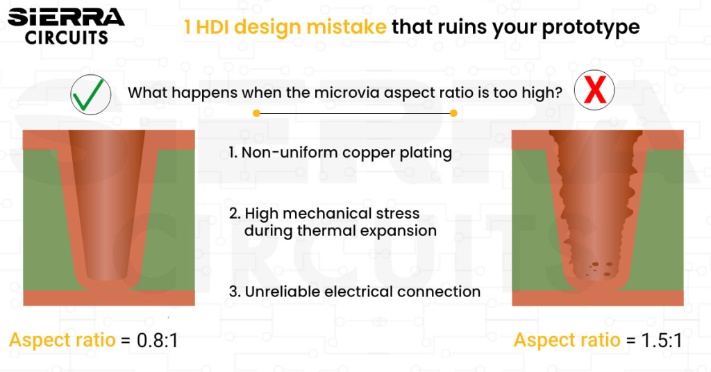
Small via geometries and higher aspect ratios can increase the risk of incomplete filling and void formation. Specialized plating chemistry and tightly controlled process parameters may be required for consistent microvia filling.
Key challenges include:
- Microvia filling: Achieving reliable and uniform copper deposition inside the microvia.
- Fine-line definition: Preventing excessive lateral plating that changes trace width or spacing.
- Current-density variation: Managing differences between isolated and densely packed features.
- Copper thickness uniformity: Maintaining consistent deposition across the panel.
- Feature interaction: Closely spaced traces, pads, and vias can influence local plating behavior.
- Process control: Chemistry, current, agitation, temperature, and plating time must be tightly controlled.
You should:
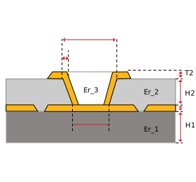
- Define microvia diameter, depth, and capture-pad dimensions within the manufacturer’s reliable plating capability.
- Avoid unnecessarily aggressive microvia aspect ratios that make reliable copper deposition more difficult and avoid hole defects.
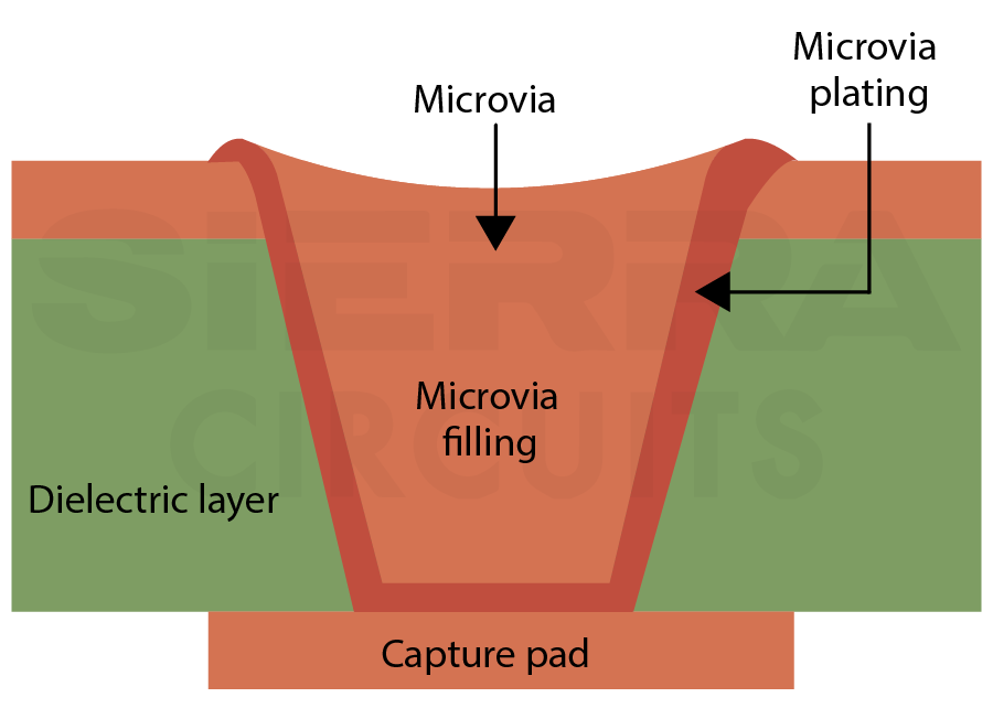
According to Steve Carney, R&D Project Manager at Sierra Circuits, “The biggest failure for laser vias is separation between the barrel/fill plating and the capture pad, resulting in opens. This problem was so prevalent that it earned the term “eyebrowing” because one side of the via remained attached and the separation would form an arc like an eyebrow.”
7. Controlling flash etching without damaging fine features
After copper is plated onto the exposed circuit pattern, the remaining seed copper between the conductors must be removed. This flash-etch step requires tight process control because the etchant must remove the unwanted seed copper without significantly reducing the plated traces.
Over-etching can reduce conductor width or thickness, while under-etching can leave copper residues that create shorts.
For SAP and mSAP designs, you should work with the fabricator to understand the qualified etch process and its effect on the final line/space geometry
8. Managing feature placement to reduce plating and etching risk
Feature placement can create both plating and etching problems. Isolated fine traces may receive insufficient plating current, particularly when they are separated from the main concentration of circuitry.
Small traces located within tight plane openings can also create confined regions where etchant can accumulate during flash etching. This can increase the risk of the trace being attacked during seed-layer removal.
Designers should:
- Avoid isolated fine-line features where the electrical design permits.
- Maintain consistent feature density where practical.
- Review narrow openings and dense-to-sparse transitions with the fabricator.
- Follow the fabricator’s recommendations for copper balancing and dummy features.
What causes yield loss in additive board manufacturing?
Mushrooming, seed etch undercut, and lithography/registration errors are the three most common causes of yield loss in mSAP PCBs, as they can alter trace geometry, reduce spacing, and create opens or shorts.
1. Mushrooming: Electroplated copper grows laterally beyond the resist opening, reducing spacing and increasing the risk of shorts. Fabricators mitigate this issue by tightly controlling the electroplating process, limiting the target plated copper thickness, and using photoresists with near-vertical sidewalls to minimize lateral copper growth.
2. Seed etch undercut: The flash etch process used to remove the seed layer between traces can over-etch if not tightly controlled, causing line necking, higher resistance, or opens. CMs minimize undercut by tightly controlling the flash etch time (typically under ~60 seconds, depending on the process chemistry) and continuously monitoring the etch rate (µm/min) to remove the seed layer without excessively attacking the trace edges. For SAP and mSAP designs, the designer should confirm the fabricator’s etch capability rather than applying a universal etch-time requirement
3. Lithography and registration errors: Misalignment during photoresist imaging or dimensional changes caused by panel expansion can shift fine features, resulting in reduced yield. Fabricators improve registration accuracy by using laser direct imaging instead of contact exposure, maintaining registration tolerances of ≤ ±12 µm, and applying X/Y scaling compensation to account for panel expansion during processing.
Need help designing your ultra-HDI boards? Our engineering team can help you with stack-up, layout planning, and DFM analysis.
To talk to a PCB expert: Book a meeting or call us at +1 (800) 763-7503.

Global and North American SAP and mSAP PCB market projections
The semi-additive process and modified semi-additive process market is experiencing rapid growth, driven by an industry-wide shift toward miniaturization. Fab houses are increasingly adopting these manufacturing techniques to meet this requirement.
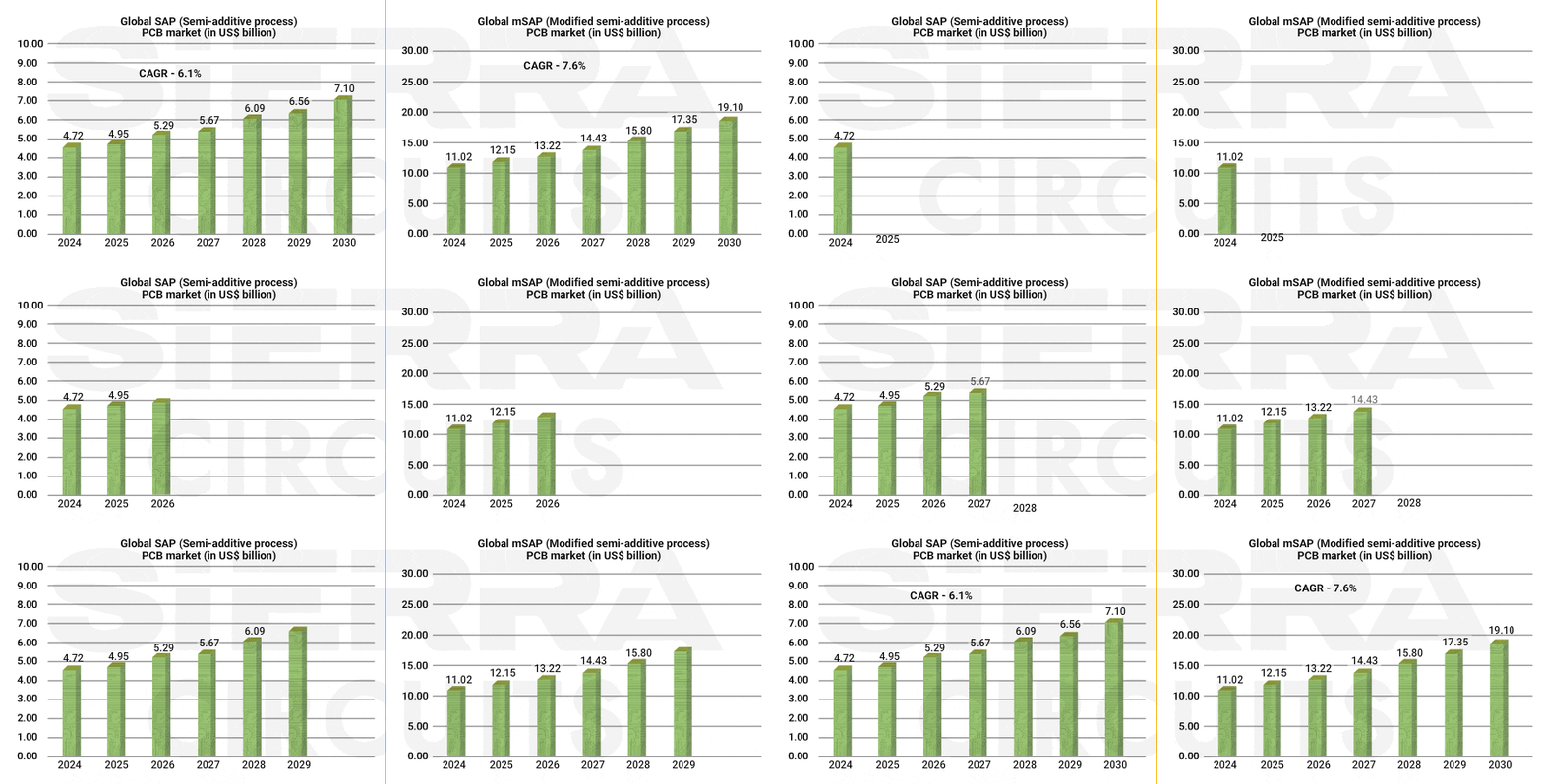
The global SAP market will reach US$ 7.10 billion by 2030, growing at a CAGR of 6.1% between 2026 and 2030. During the same period, the global mSAP market will reach US$ 19.10 billion, at a CAGR of 7.6%.
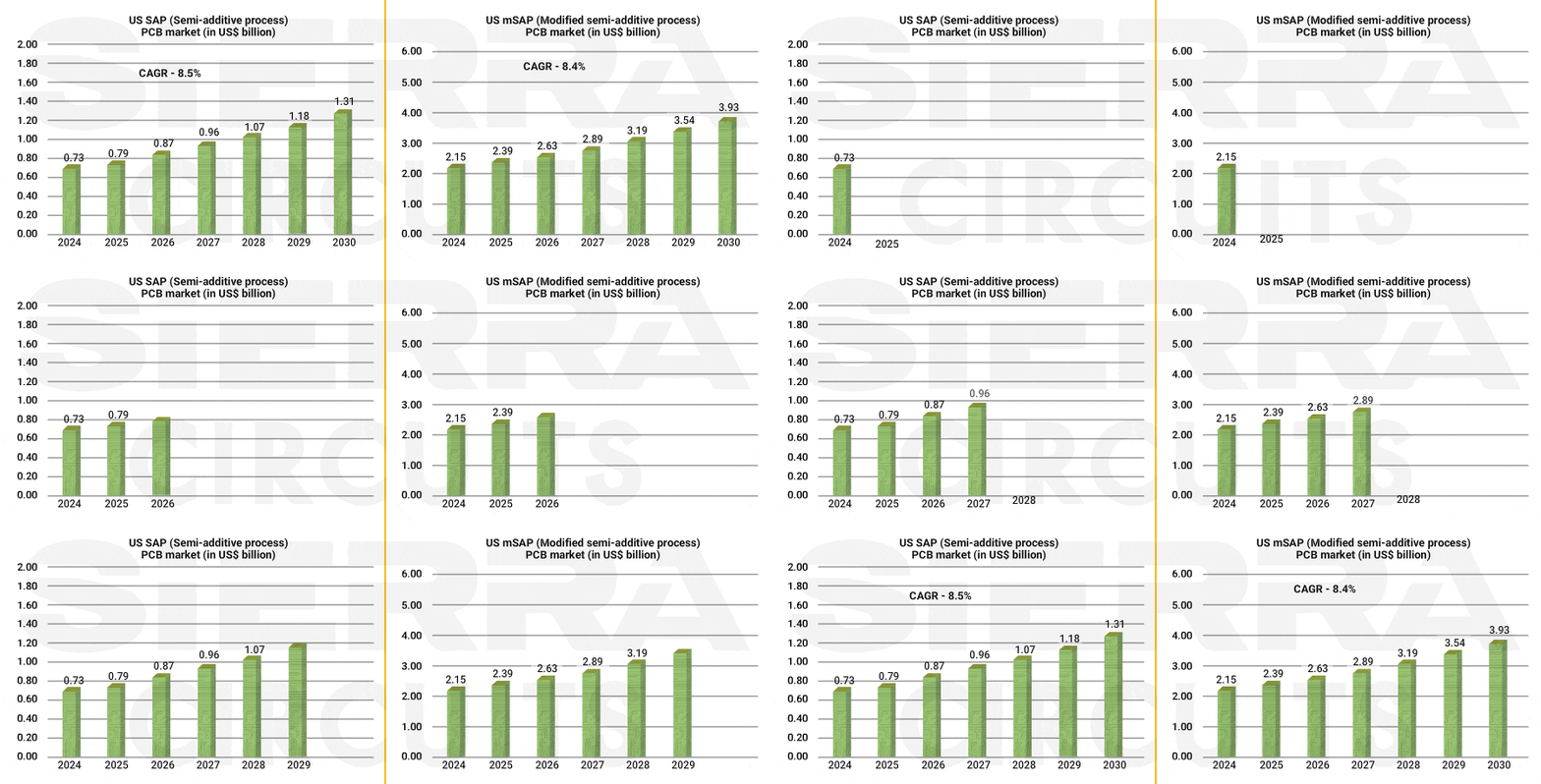
The North American SAP market will reach US$ 1.31 billion by 2030, growing at a CAGR of 8.5% between 2026 and 2030. During the same period, the North American mSAP market will reach US$ 3.93 billion, at a CAGR of 8.4%.
Source: Sierra Circuits’ market research analysis report.
SAP and mSAP PCB manufacturing technologies enable routing densities that are difficult to achieve with conventional subtractive etching. By building copper additively, these processes improve dimensional control, impedance consistency, and fine-pitch routing capability.
Successful implementation depends on early stack-up planning, right material selection, and process-aware design practices. Defining additive layers during the layout stage helps improve yield and avoid expensive redesigns.
About Mohamed Faheemuddin : Mohamed Faheemuddin is a mechanical engineer. His passion for electronics drew him to the PCB industry. With an experience of over 3 years in the PCB industry, he specializes in developing articles for engineers and hardware designers.





Start the discussion at sierraconnect.protoexpress.com