UHDI PCB Design and Manufacturing
Sierra Circuits' UHDI PCB Design and Manufacturing guide helps you build ultra-high-density boards using advanced additive fabrication technologies.


The UHDI PCB Design and Manufacturing guide covers material and stack-up considerations, layout development, and DFM principles for creating reliable ultra-high-density interconnect (UHDI) PCBs.
Here’s a quick breakdown of what you’ll learn in this design guide:
- What defines an ultra-HDI PCB and how fine features and thin dielectrics increase routing density
- Overview of SAP, mSAP, and embedded trace technology that enable 2/2 mil trace geometry
- How to decide whether your design requires additive fabrication
- Choosing materials for dimensional stability, laser processing, and consistent electrical performance
- How to develop ultra-HDI stack-ups that withstand multiple lamination cycles with accurate layer-to-layer registration
- Manufacturing challenges that impact UHDI yield
- DFM guidelines for optimizing ultra-high-density interconnects for manufacturability and reliability
- Questions to ask a PCB fabricator about process capability, registration, materials, and production limits
What are UHDI PCBs?
Ultra-HDI interconnects are advanced circuit boards that use extremely fine traces and spaces, small microvias, and thin dielectric layers to achieve higher routing density. These prototypes feature fine traces and spaces (≤50 microns or 2 mil), small-diameter microvias (<100 microns), and thin dielectric layers that reduce parasitic effects and support high-speed signaling.
It is an extension of standard HDI; the fundamental difference lies in the tighter geometries and higher routing densities. These geometries make UHDI PCB design and manufacturing more sensitive to variations in imaging, drilling, lamination, plating, and layer-to-layer registration.
For example, a conventional layout may allow an 8 mil drill-to-copper clearance, whereas an ultra-high-density design may require only 4 mil. This demands much higher positional accuracy during drilling and lamination.
As feature sizes shrink, maintaining adhesion, material integrity, and dimensional stability becomes increasingly challenging. Ultra-HDI PCB designs therefore require tightly controlled fabrication processes, often incorporating sequential lamination and additive technologies. These processes build copper only where circuitry is needed. They also provide greater control over trace width, spacing, and sidewall geometry than conventional subtractive fabrication.
Why use additive fabrication for fine board features?
The manufacturing process directly influences the minimum feature sizes that can be reliably achieved on a PCB. Traditional subtractive etching starts with a thick copper-clad laminate and chemically removes unwanted copper. This approach inherently causes etch undercut, resulting in trapezoidal trace cross-sections that negatively impact impedance control and signal integrity. At very low line widths (<2 mil), maintaining yield and consistency becomes increasingly difficult.

Semi-additive process (SAP) and modified semi-additive process (mSAP) address these limitations by depositing copper additively rather than etching it away. SAP begins with an ultra-thin sputtered seed layer, while mSAP starts with a thin laminated copper foil (~1.5 microns).
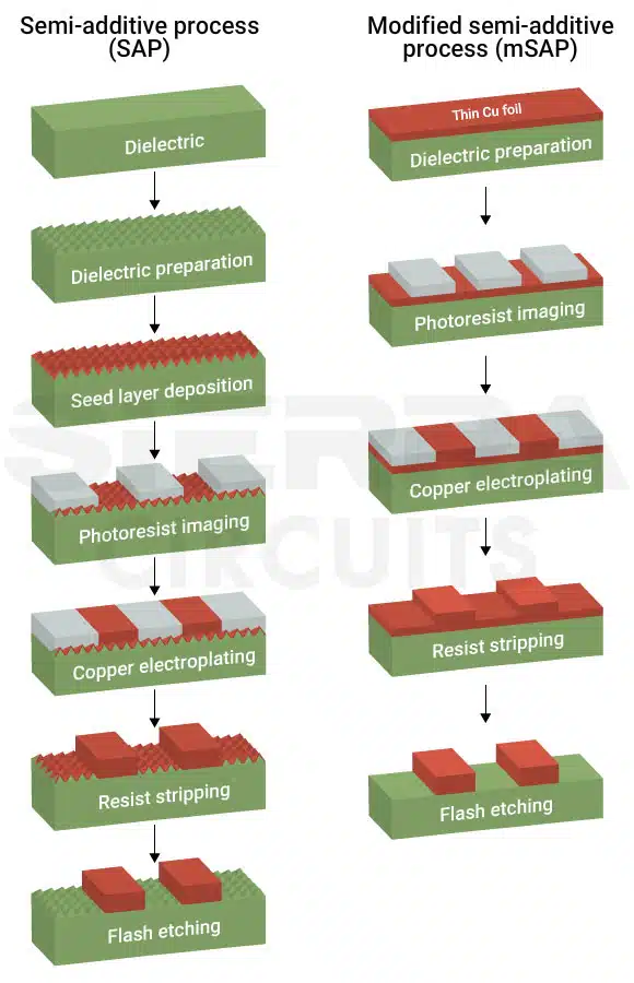
In both methods, photoresist defines the circuit pattern, and electrolytic copper is plated to the required thickness. A brief flash etch then removes the minimal base copper between traces. This additive approach yields near-vertical sidewalls, minimizes undercutting, and ensures precise dimensional control, making it ideal for UHDI PCB manufacturing.
Embedded trace technology provides another approach by forming copper conductors within trenches created in the dielectric. The process can improve trace stability during lamination and produce smoother conductor surfaces that can reduce high-frequency conductor losses.
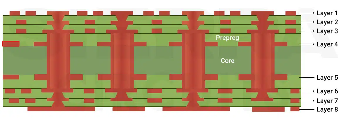
For a multilayer PCB, additive technology does not necessarily need to be used on every layer. High-density signal layers can use an additive process where fine geometries provide a routing benefit, while conventional subtractive processing can be used on power, ground, or standard-routing layers where ultra-fine features are not required.
When should you consider UHDI for your design?
A design needs fine-feature technology when its routing density, component pitch, microvia geometry, or electrical requirements cannot be met reliably with conventional fabrication. Not every advanced PCB requires ultra-HDI; the manufacturing process should be selected based on the actual design requirements.
Start by identifying the most demanding area of the layout. Fine-pitch BGA packages are a common driver because more I/Os must escape from a smaller component area as package pitch decreases.
Consider these factors:
- Minimum trace width and spacing
- Component pitch and BGA breakout
- Microvia diameter and capture-pad size
- Signal integrity and impedance requirements
- Copper thickness and current needs
- Stack-up and layer count
- Production volume
- Manufacturing cost
- Fabricator capabilities
For example, routing 2-mil traces may require laser-drilled microvias with a diameter of 75–100 microns and a capture pad of 200 microns. These trace, via, and pad dimensions should be considered together to ensure adequate space for reliable routing and fabrication.
Select the simplest manufacturing process that satisfies the design. In some prototypes, an additive process is needed only on high-density signal layers, while conventional subtractive fabrication can remain on power, ground, and lower-density layers.
How does material selection affect ultra-HDI PCB manufacturing?
Laminates must provide the dimensional stability, glass structure, resin behavior, and laser compatibility required for fine-feature fabrication. Even small variations in material movement, dielectric thickness, or glass structure can impact registration, interconnect reliability, and manufacturing yield.
Laminates such as Tachyon 100G, Panasonic Megtron 6, EM-528, and EM-892K are primary choices for UHDI with mSAP. Higher-end materials from manufacturers such as Isola, Panasonic/Megtron, EMC, and Ventec can also be considered.
Glass structure is as important as the resin system. Spread or flattened glass constructions are preferred because their uniform yarn distribution provides greater dimensional stability during lamination and improves resistance to conductive anodic filament (CAF) formation. Standard woven glass creates localized high points where yarns overlap, leading to resist bridging and undercut during fine-line imaging. Flatter glass styles, such as 1035, 1067, and 1086, provide a uniform surface for high-resolution resist and support cleaner laser ablation for microvias.
Material selection should therefore consider more than Dk, Df, or resin family. You should evaluate:
- Glass style and structure
- Resin content and pressed dielectric thickness
- Dimensional stability
- Laser-drilling compatibility
- Microvia diameter and aspect ratio
- Electrical properties
- Fabricator’s sequential-lamination process
Copper foil roughness is another critical consideration at high frequencies. Smoother copper reduces conductor loss but weakens mechanical adhesion. Rougher copper surfaces increase signal loss, so use very-low-profile (VLP) and reverse-treated foils (RTF) to reduce this effect. However, overly smooth copper on fine 2-mil traces can weaken adhesion and cause traces to shift during lamination. Foil selection must carefully balance signal-loss targets, trace geometry, and fabricator capability.
How to build a manufacturable UHDI stack-up?
Plan an ultra-HDI layer stack around routing density, microvia architecture, lamination sequence, material movement, and the fabricator’s registration capability. Since fine traces and small microvias leave very little positional margin, consider registration early in the design process.
Start by defining the core and build-up layers and identifying which layers require fine-line processing. Avoid unnecessary sequential lamination cycles because each additional cycle introduces another possibility for material movement and registration variation.
Microvia geometry should also be matched to dielectric thickness. Maintain a 0.8:1 microvia aspect ratio to provide a greater process window for laser drilling and plating. Prefer staggered microvias over stacked ones because stacked structures require additional processing and can introduce greater mechanical stress.
A hybrid stack-up can be useful when only certain layers require ultra-high-density interconnect features. Assign the additive process to dense signal layers and use the subtractive process for power planes, ground planes, or standard routing.
Maintain a balanced copper distribution across the build-up to prevent warpage. Copper distribution can influence material movement during lamination, making registration an important consideration for fine-feature layers. Utilize subassembly-based approaches for high-layer-count designs. This divides complex multilayer constructions into controlled manufacturing stages.
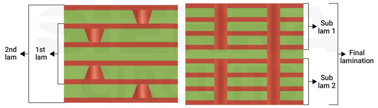
Always verify that your CM utilizes advanced scaling compensation systems, such as predictive software and internal target fiducials, to track and correct material movement during production.
Sierra Circuits uses XACT, a self-learning system for predicting and tracking material movement. It has accumulated around 260,000 data points in its database. The system uses reference-build data to establish and refine scaling values for different constructions.
What causes yield loss in UHDI manufacturing?
Ultra-HDI technology has a smaller process window because even small variations can change trace dimensions, spacing, registration, or microvia reliability.
Three major causes of yield loss are:
- Mushrooming: Plated copper can grow laterally beyond the resist opening, reducing spacing and increasing the risk of shorts.
- Seed-etch undercut: Excessive flash etching can reduce conductor width or cause line necking, while insufficient etching can leave copper residues between traces.
- Lithography and registration errors: Imaging misalignment and panel movement can shift fine features and reduce available spacing.
Other manufacturing challenges include seed-layer uniformity, resist thickness, current-density variation during plating, microvia filling, copper-thickness control, and feature placement.
For this reason, you should work with the fabricator’s proven process window rather than designing only to a theoretical minimum.
What DFM guidelines should you follow for ultra-HDI PCB designs?
Achieving 2/2 mil features requires strict adherence to design for manufacturing guidelines. Follow these rules to ensure manufacturability:
- Limit the total board layer count to 16 layers.
- Use 2/2 mil technology on no more than 4 layers.
- Keep copper plating on 2/2 mil layers at or below 25 microns (1 mil).
For more pointers, download the full design guide.
The manufacturer should review the design before fabrication to confirm that the selected stack-up, materials, copper thickness, via structures, clearances, and special features fall within the qualified process window.
What should you ask a PCB manufacturer before starting a UHDI design?
Ask the fabricator for production-proven process capability rather than relying only on equipment specifications or theoretical minimums. Fine-line manufacturability depends on what the manufacturer can consistently achieve across actual production panels.
Before starting your design, ask:
- How do you measure and compensate for material movement?
- What layer-to-layer registration tolerance can you reliably achieve?
- What line/space can you consistently manufacture?
For more, download the full design guide.
These questions help establish the actual process window before routing begins.
Sierra Circuits is constantly adding and upgrading process equipment to keep up with advancing technology. The latest tech additions include dry film lamination, vacuum lamination, direct imaging, mechanical vision drilling, laser drilling and routing, plasma, etching, copper plating, electrical testing, and in-process/final inspection.
As trace widths get smaller, the process windows shrink as well, so we have developed an extensive system to monitor and control every process, chemistry, and piece of equipment we use to ensure it’s running at the optimum level. This enables us to consistently deliver high-quality product to our customers when they need it. We implement the mSAP on the layers that require 2/2 mil traces.
Download the UHDI PCB Design and Manufacturing guide to learn how to plan your stackup, layout, and manufacturing process for building ultra-high-density circuit boards.