


Contents

On-demand webinar
How Good is My Shield? An Introduction to Transfer Impedance and Shielding Effectiveness
by Karen Burnham
Ground bounce in PCBs poses significant signal integrity issues, such as false switching, timing errors, and EMI. As a PCB designer, understanding the causes of ground bounce helps you apply the right grounding techniques to minimize noise and ensure reliable performance.
Highlights:
- Proper grounding techniques, such as continuous ground planes and shielding of chassis, help you suppress ground bounce.
- Common layout mistakes, like inadequate ground vias or split ground planes, can lead to ground loops and noise issues.
- Place bypass capacitors close to IC supply pins with short and wide traces to reduce noise in your boards.
In this article, you’ll learn the cause, effects, and prevention techniques of ground bounce.
What is ground bounce in PCBA?
Ground bounce is a type of electrical noise or voltage fluctuation that occurs in the ground plane of a circuit board. It is generally caused by parasitic inductance, transient effects, poor grounding, or inadequate decoupling.
Ideally, the voltage between an IC’s supply and ground pins should match the voltage of the corresponding supply and ground points (planes) on the PCB. Ground bounce occurs when there is a mismatch between these voltages.
How do you ground a circuit board properly?
In large electrical systems, like substations and transmission equipment, the return path for current is directly connected to the physical ground. This method is termed direct grounding. Many of the electronic circuits lack this provision.
In applications like automobiles or space vehicles, printed boards are electrically isolated from the physical ground. To ensure proper current return paths, designers create designated points or planes on the PCB that are maintained at ground potential. This approach is known as indirect grounding.
Here are the different grounding methods used in circuit design:
1. Chassis ground
A common ground point connected to the metallic enclosure of a device is called chassis ground. All the ground points across a PCB come together to connect at this point. It provides electric shock protection and physical shielding to the device. The chassis ground prevents the current flow through the entire surface area of the chassis. This eliminates EMF-induced ground loops.
2. Signal ground
Signal ground is a point on the board from where the signals are measured. It is usually on the surface of the board and connects to an internal ground plane. There are chances of noise injection/interference occurring at these signal ground points. That is why these points are placed on the PCB itself and not isolated to a different location.
Cleaner signal grounds are an essential parameter when it comes to boards that deal with accurate low voltages. In these circuit boards, even small noise signals create signal integrity issues.
Analog and digital parts of the same circuit board can share the same signal ground.
Download our design guide to learn how to build high-speed PCBs with signal integrity.

High-Speed PCB Design Guide
8 Chapters - 115 Pages - 150 Minute ReadWhat's Inside:
- Explanations of signal integrity issues
- Understanding transmission lines and controlled impedance
- Selection process of high-speed PCB materials
- High-speed layout guidelines
Download Now
3. Ground plane
Ground plane is a layer on the PCB stack-up maintained at 0 potential. It acts as a plane for reference and a sink for return currents circulating through the board. Signal ground points from the surface are connected to the ground plane through vias.
A ground plane provides an efficient signal return, voltage return, and reduces noise and interference. It is a good practice to keep the ground planes continuous. This will avoid the formation of ground loops that offer an alternative current return path, thereby disrupting the operation.
4. Earth ground
It is a direct connection from the circuit to the physical ground. Earth ground is prominent in electronic appliances.
A short-circuit in the electrical interconnect or a live component in contact with the chassis/covering of the equipment is dangerous. Operating personnel will be electrocuted by touching the chassis. Therefore, all the high-voltage circuits require an earth ground.
What causes ground loops?
Ground loops are multiple current return paths caused by fluctuations in the ground potentials throughout the circuit. Thus, the current circulates through other shorter paths than the desired path.
Ideally, all the ground points and planes on a PCB assembly should be at the same potential. But in real scenarios, there is inductance in the leads that connect the IC to the board. This inductance creates small voltage drops and becomes the reason for the ground bounce.
The induced parasitic inductance is very small in value, but cannot be ignored for devices like transistors. These devices are high-speed switching circuits made of logic gates. The signal voltages of transistors switch between high 1 and low 0.
When the IC voltage is at 1, it means that the output voltage is approaching VCC. Similarly, if the voltage is at 0, it indicates that the output voltage is approaching the ground potential (0 V). Due to the inductance mentioned above, the ground voltage starts fluctuating or bouncing to different values other than 0 V. This is the reason behind ground bouncing.
Ground bounce causes the circuit to misinterpret low (0) as high (1). Thus, the operation of digital logic devices throughout the board is affected.
Apart from the effect on the operations, ground bounce is regarded as noise on the PCBA, which in turn degrades signal integrity. To mitigate this effect, designers follow established guidelines to minimize or eliminate ground bounce.
6 layout mistakes that lead to ground loops
Below are common layout mistakes that often result in ground loops:
- Routing RF signals over gaps/slots in ground planes.

An illustration showing splits in the ground plane. This might cause impedance discontinuities in RF boards. - Inadequate ground vias between layers create high-impedance return paths.
- Isolated ground pads or polygons not tied to ground planes.
- Not connecting cans, shields, or metal enclosures to the ground planes.
- Using thin traces instead of solid copper pours for grounding.
- Sharing the RF ground with noisy circuits like switching power supplies or microcontrollers.
For more high-speed design tips, watch the full webinar here: Designing ultra-linear RF.
How is ground bounce generated?
The generation of ground bounce can be clearly explained using a circuit like the one given below.

The figure shows a circuit with a CMOS connected to an output load with CL capacitance and RL resistance. Other parameters are given below:
- LA: intrinsic inductance in the power lead of the package
- LB: intrinsic inductance in the output lead of the package
- LC: intrinsic inductance in the ground lead of the CMOS package
- R1: output resistance of the CMOS IC
Let’s consider a scenario when the output changes from high (1) to low (0). In such a case, the current flows out of the load side, and the load capacitance discharges.
The flow of this current (i) across the inductances LB and LC generates a voltage, V= L(di/dt). This generated voltage causes the potential of the internal CMOS ground to be different from that of the external load ground.
Thus, the internal reference ground is at a higher potential compared to the zero potential of the external ground. This difference appears as the noise in the circuit and affects the operation of the switching devices in the circuit.
The ground bounce oscillations of a circuit observed through an oscilloscope are shown below.

The top waveform represents the output of the I/O pins of the switching device. The bottom waveform shows the spikes (noise) due to ground bounce.


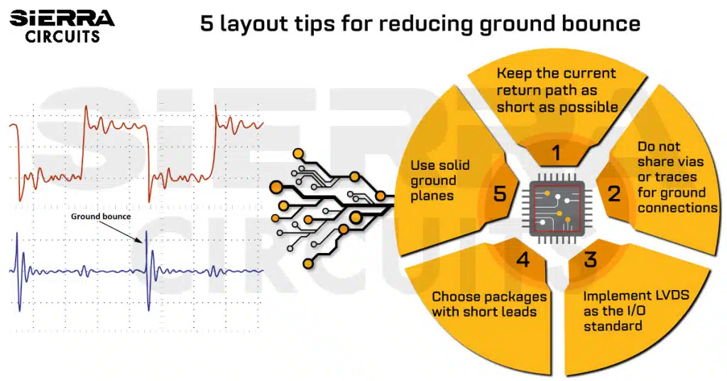
How to reduce ground bounce
Stick to these layout rules to lower ground bounce in your circuit board designs:
7 layout design rules for ground bounce reduction
- Use via-in-pads wherever possible as permitted by the design.
- Reduce the signal return path distances. The reduced distance will decrease the parasitic capacitance. To achieve this, it is best to place the components right above their ground points.
- Never share ground vias or traces for ground connections. It is recommended to use individual vias and traces to connect to the ground plane.

Recommended ground connections. - Do not connect capacitors directly to the outputs.
- Implement low-voltage differential signaling (LVDS) as the I/O standard. This standard offers high bandwidth and high noise immunity.
- Choose packages with short leads to reduce the series inductance. BGAs are also recommended.
- Use solid ground planes to reduce IR losses and inductance. Avoid ground split planes.
What does a bypass capacitor do?
The most common method to reduce ground bounce is to place a bypass capacitor on the circuit. A bypass capacitor effectively bypasses the voltage spikes and power supply noises. It is connected between the VCC and GND pins of an IC package.
A capacitor behaves differently in AC and DC circuits. In DC circuits, it gets charged to the supply current and then blocks the flow of current completely.
In AC circuits, it provides an easy path for the transient signals to the ground. Thus, ground bounces or noises that are transient signals are bypassed directly to the ground. The DC signals will be blocked by the capacitor and, hence, flow through the circuit and facilitate the operation.

To ensure effective noise suppression, consider the following guidelines when selecting a capacitor:
- Lead inductance: Keep it minimal, as higher inductance can reduce the capacitor’s ability to suppress high-frequency noise.
- Capacitor type: Multilayer ceramic chip capacitors (MLCCs) are preferred due to their low ESL (equivalent series inductance) and excellent high-frequency performance.
- Maximum capacitor current: Choose a capacitor that can handle the peak current determined by the maximum pulse slew rate.
- Load current switching: Consider the amount of current drawn during low-to-high transitions, as it influences the required capacitance value and placement.
Where should a bypass capacitor be placed on a PCB?
A bypass capacitor is placed as close to the supply pin of the component as possible. This capacitor acts as local charge storage for the switching components, like transistors. The additional voltage spikes are stored in this capacitor and not circulated through the circuit.
Therefore, all the ground points will have the same potential, and ground bounce noises do not appear. Here are some more design guidelines related to bypass capacitors:
- Use wide and short traces and vias to connect the bypass capacitor pads to power and ground pins. This minimizes inductance and improves the current flow.
- Incorporate SMD capacitors.
- Add vias close to the capacitor pads.
Ground vias, dedicated ground planes, and galvanic isolation are essential PCB grounding techniques in high-power/HDI boards.
What is the difference between bypass and decoupling capacitors?
Capacitors are widely used as bypass and decoupling components. These terms are extremely common in circuit board designs, and hence, let’s have a look at the differences between the two.
| Bypass capacitor | Decoupling capacitor |
|---|---|
| Bypasses noise signals to the ground | Seperates two circuits from each other |
| Placed between the supply voltage and ground pins | Placed in parallel to the power supply and the load |
| Shorts AC signal to the ground | Creates a low impedance path for high-frequency signals |
Key takeaways
- Ground loops occur when multiple return paths exist due to potential differences, creating unwanted current circulation.
- Ground bounce is generated by parasitic inductance in IC package leads, causing voltage fluctuations.
- Bypass capacitors help suppress ground bounce by diverting transient signals to ground.
- Additional reduction techniques: solid ground planes, via-in-pad, dedicated ground vias, short signal return paths, and choosing low-inductance packages.
Ground bounce reduction techniques result in better signal integrity. These methods remove all the transient noises in the circuit and thus increase efficiency.
Download our design guide to learn how to build a reliable PCB stack-up.
PCB Stack-Up Design Guide
12 Chapters - 55 Pages - 60 Minute ReadWhat's Inside:
- Design guidelines for HDI, flex, and hybrid stack-ups
- Stack-up representation in fab drawing
- DFM checks for layer stacks
- Characteristics of high-speed materials
- Manufacturing tolerances
- PCB stack-up examples with illustrations
Download Now
Have questions about printed circuit boards? Post your queries on SierraConnect. Our PCB experts will answer them.

About Pooja Mitra : Pooja Mitra is an electronics and communication engineer. With an experience of over three years in the PCB industry, she creates industry-focused articles that help electrical and PCB layout engineers.


Start the discussion at sierraconnect.protoexpress.com