


Contents

On-demand webinar
How Good is My Shield? An Introduction to Transfer Impedance and Shielding Effectiveness
by Karen Burnham
Key design strategies for enhancing microvia reliability include selecting suitable materials for laser drilling, adhering to IPC-T-50M guidelines, and implementing stack-up configurations in alignment with IPC-2226 standards.
Microvia failure occurs due to the thermal stresses that arise during the PCB assembly process. These stresses can have a significant impact on the reliability of the plated hole.
Highlights:
- Factors contributing to microvia failures include the use of high-temperature dielectric materials and expansion rate mismatch during reflow.
- IPC-TM-650 2.6.27 and 2.6.7.2 methods offer comprehensive microvia testing procedures.
- The change in microvia resistance during the reflow cycle should not exceed 5% of the initial value.
In this article, you’ll learn the factors that lead to microvia defects, the reasons they fail during reflow, and practical design tips to improve their reliability.
2 primary factors that contribute to microvia failure
Microvia defects mainly occur due to the expansion rate mismatch, and multiple lamination cycles. Let’s look at these factors briefly:
1. Expansion rate mismatch
The discrepancy between the expansion rates of glass epoxy and copper during the reflow process, with glass expanding 200 parts per million and copper expanding 16 parts per million, results in connection failure in the microvia.
2. Multiple lamination cycles
HDI circuit boards may undergo multiple PCB lamination cycles and potentially affect the durability of the plated holes. This is due to continuous exposure to the high temperature and pressure during the lamination process.
For strategies to build reliable high-density boards, download the HDI PCB Design Guide.

HDI PCB Design Guide
5 Chapters - 52 Pages - 60 Minute ReadWhat's Inside:
- Planning your stack-up and microvia structure
- Choosing the right materials
- Signal integrity and controlled impedance in HDI
- Manufacturing considerations for higher yields
Download Now
What leads to microvia failure during the reflow process?
Microvias fail when the dielectric material and copper expand at different rates during reflow. It causes separation at the capture-pad or target-pad interface.

Commonly observed microvia flaws include:
- Barrel cracks
- Corner crack between the capture pad and the target pad
- Target pad pull-out
- Misregistration of the ablated hole to the target pad
- Misregistration of the ablated hole to the capture pad
- Copper void in filled microvia
When the board undergoes thermal excursions during the reflow process, there will be an expansion in the z-axis. Due to the dissimilar CTEs of copper and the dielectric material, they expand at different rates. This causes separation at the microvia interfaces. This dislocation may not result in an immediate failure but could become latent.

These microvias open up when the temperature rises above Tg and close or self-heal when the temperature gets below Tg. Since these separations or cracks self-heal, the only way to identify them is to monitor the resistance of the microvia through the entire temperature cycle to observe that failure mechanism. IPC-TM-650 2.6.27 method helps manufacturers carry out microvia reliability testing using D-Coupons. We will discuss more about D-coupons in an upcoming section.
To know more about the via protection method via tenting, read PCB via tenting design rules and fabrication notes.
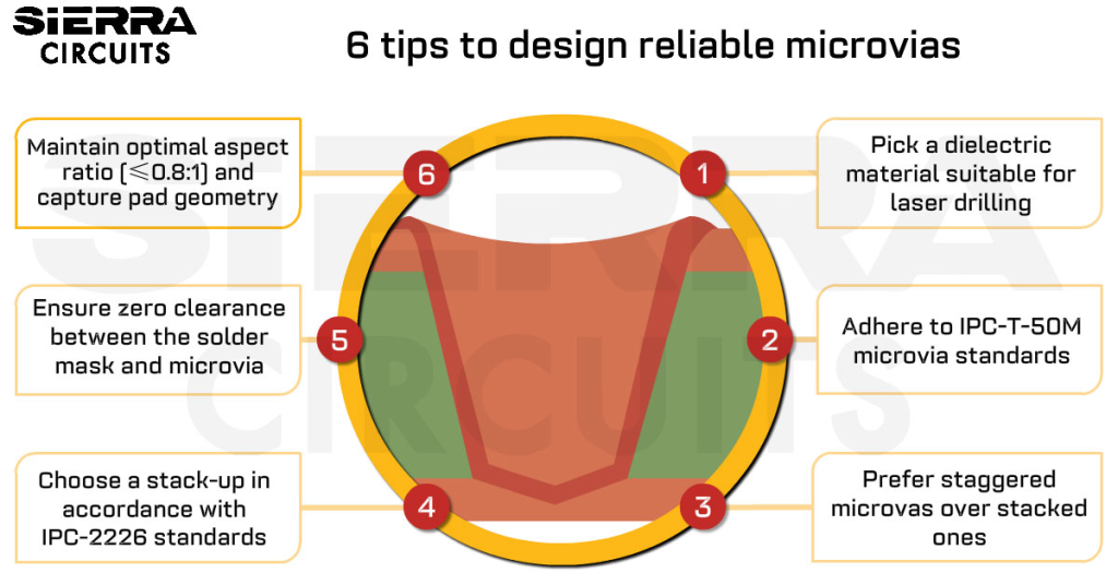
6 tips to design reliable microvias
1. Pick a dielectric material suitable for laser drilling
Dielectric materials must be laser drillable and compatible with sequential lamination cycles. High-quality resin systems with flat or spread glass structures are suitable for laser drilling. The glass structure directly affects drilling quality, plating adhesion, and thermal expansion behavior during reflow cycles.

Stick to these guidelines when choosing materials:
- Choose laser-drillable resin systems with flat or spread glass styles (e.g., Isola FR408HR, FR370HR, I-Speed, Nelco N7000-2HT). These provide a more homogeneous surface for consistent laser ablation and reduce the risk of glass fibers protruding into the via.
- Maintain high stack-up homogeneity, as different materials absorb laser energy at different rates. This prevents uneven heating, material charring, and inconsistent via taper.
- Prefer dielectric materials with flat or spread glass (1035, 1067, 1086) with thickness kept to a minimum. These types of glass structures are more stable than standard glass and help reduce the amount of stress put on the micro-via structure especially at the capture pad interface.
- Adopt non-reinforced or minimally reinforced build-up films (e.g., ABF) for advanced HDI to achieve clean laser drilling, low z-axis expansion, and high stacked-via reliability.
Check out Sierra Circuits’ Material Selector for more such application-specific materials.

2. Adhere to IPC-T-50M microvia standards
IPC-T-50M defines key geometric limits that ensure manufacturable and reliable microvias. Follow these constraints during layout:
- Maintain a maximum aspect ratio of 1:1 to ensure uniform plating and prevent thin copper at the via bottom.
- Limit microvia diameter to 6 mil to avoid drilling instability and taper variation.
- Keep the capture-pad to target-pad distance ≤10 mil for predictable laser depth control.
3. Prefer staggered microvias over stacked ones
Staggered microvias reduce vertical stress accumulation and survive more thermal cycles than stacked vias.
Keep these things in mind when designing microvias:
- Maintain a vertical offset greater than the via diameter between adjacent microvias to prevent barrel overlap.
- Apply a minimum 2 mil spacing between staggered structures for drill stability and plating flow.
- Fill only the external-layer microvias when staggering. This reduces the cost while preserving structural reliability.
- Use stacked microvias when routing density is extremely high (e.g., fine-pitch BGAs) and layer-to-layer registration is critical. If the board space is tight, stacked 1-2 and 2-3 microvias allow much smaller diameters (4–5 mil), but they increase the cost.
- Implement skip vias when you need to connect layers 1, 2, and 3 without extra lamination steps, and when larger mechanical drill sizes (8-10 mil) are acceptable. Laser drilling isn’t suitable here because the energy needed to break through the layer 2 capture pad can cause delamination.

- If you want to connect two layers, say 1 to 2, then a non-filled laser via would be more affordable. If multiple layers need to be connected, then a mechanically drilled via-in-pad would be cost-effective. However, you should also consider the tradeoff between space and cost considerations.
To learn more about stacked and staggered microvias, see design and manufacture of staggered and stacked vias in PCBs.
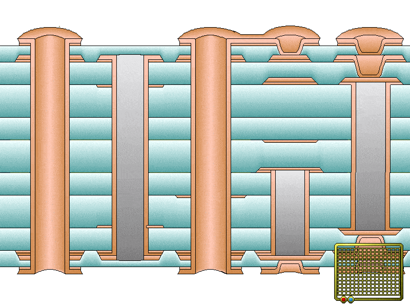
4. Choose a stack-up in accordance with IPC 2226 standards
IPC-2226 defines standard HDI build-up types to ensure the manufacturability of your microvias and cost-efficient production. The images below depict the stack-up structures conforming to IPC-2226 standards. These structures ensure efficient heat dissipation and prevent thermal stress on the microvias.
IPC-2226 type I
This configuration features a PTH and a single microvia layer on either one or both sides of the core.

IPC-2226 type II
It has a PTH, buried via, and one microvia layer on one or both sides of the core.

IPC-2226 type III with stacked microvias
Type III configuration has a PTH buried via and at least two layers of microvias on either one or both sides of the core.

IPC-2226, type III with staggered microvias

Features a PTH, buried via, and at least two microvia layers on at least one side of a core with staggered microvias.
IPC-2226, type III, with filled, capped, and staggered microvias
This configuration features 2 PTHs with one of the holes capped. It has a buried via with capped staggered microvias on the outer layers.

5. Ensure zero clearance between the solder mask and microvia
Correct solder-mask clearance prevents solder wicking into microvia edges and avoids bridging during reflow.
DFM guidelines:
- Specify 0 mil solder-mask expansion around microvias to prevent solder flow into via edges.
- Avoid partial or slotted mask openings, as they trap flux and create conductive residues.
- Confirm your fabricator’s mask registration tolerance (typically ±2-4 mil) before requiring tight mask alignment on outer layers.
- This ensures clean pad definition and reduces reflow-related solder defects.

Zero clearance between the microvia and the solder mask.
6. Maintain optimal aspect ratio (≤0.8:1) and capture pad geometry
Microvia plating reliability depends on aspect ratio and pad geometry.
- Keep the target pad diameter (bottom of the via) at least 80% of the via diameter to reduce stress concentration at the interface. This also helps to texture the target pad copper for better plating adhesion.
- Limit aspect ratio to ≤0.8:1. Deep, narrow vias are prone to plating voids and become crack-initiation points during reflow.

3D laser microscope image of a 6 mil laser via with straight sides and a textured target pad.
For more DFM guidelines, download the Design for Manufacturing Handbook.

Design for Manufacturing Handbook
11 Chapters - 96 Pages - 90 Minute ReadWhat's Inside:
- Annular rings: avoid drill breakouts
- Vias: optimize your design
- Trace width and space: follow the best practices
- Solder mask and silkscreen: get the must-knows
Download Now
Test coupons for testing microvias
D coupons, designed in accordance with IPC-2221 Appendix A or B, are the primary test structures used to verify microvia reliability under thermal and electrical stress. They contain long, plated-via or plated-hole chains that enable precise resistance measurements during stress testing.
These coupons are manufactured alongside the main PCB using the same stack-up and via structures as the board. This ensures that any microvia defects, plating issues, or structural weaknesses appear in the coupon exactly as they would in the board.
D coupons are suitable for all major microvia reliability test methods, including:
- HATS (IPC-TM-650 2.6.7A)
- Current-induced thermal cycling
- Micro-etch evaluation
- IPC-TM-650 2.6.27 thermal stress tests
Test coupons are typically small sections (around 200 × 30 mm) placed on the production panel. Depending on your panel strategy, they may be located in a dedicated coupon area, embedded within the main layout, or designed as separate units. These coupons allow manufacturers to simulate reflow, apply thermal shock, and perform electrical stress testing before producing the final PCB.

D coupons feature two nets that represent the plated holes and via structures from the actual PCB. They can include A/B patterns or propagated structures such as blind vias, buried vias, stacked microvias, and filled through-holes. This makes them suitable for evaluating microvia reliability across all common via transition types used in HDI designs.
During testing, a D coupon is considered failed if the resistance of the via chain increases by more than 5% during thermal cycling. This threshold is critical because microvia cracks or fractures often self-heal as the coupon cools, making failures undetectable at room temperature.
Fab notes to communicate microvia test requirements
Include these points in your fab notes if you wish to test the durability of the microvias present in your design:
- The purpose of the D-coupons is to test the reliability of plated holes.
- Hole sizes, plating requirements, and spacing between the copper features.
- Number of test coupons and the desired location on the PCB panel.
IPC-TM-650 test methods for microvia reliability
IPC, in collaboration with various OEMs and the D-32 Thermal Stress Test Methodology Subcommittee, has introduced IPC-TM-650, method 2.6.27, and IPC-TM-650, method 2.6.7.2 test methods for assessing the reliability of electrical interconnections.
These methods involve measuring the electrical resistance of test coupons at different temperatures. In method 2.6.27, the procedure involves subjecting the test coupon to a standard solder paste reflow profile designed to achieve a peak temperature of either 230°C or 260°C.
The system monitors the resistance of the coupon as you run it through the thermal cycle. The D coupon remains connected to a 4-wire resistance measuring unit throughout this process. The connection is maintained for a total of six full reflow profiles. In method 2.6.7.2, D coupons are subjected to a minimum of 6 reflow simulations and 100 thermal shocks from -55°C to 210°C.
The resistance should not increase by more than 5% during this testing phase. If this is not achieved, the device under test is considered failed.
During the reflow simulation, resistance measurements will be monitored at least every second and once every cycle during thermal shock. By implementing this testing technique, OEMs have the ability to identify and address latent microvia failures. This helps safeguard their products against potential defects that may go unnoticed.
Key takeaways:
- Microvia failures typically occur at the interfaces between the target and capture pads.
- Adherence to IPC-T-50M microvia standards is crucial to designing a reliable microvia.
- Prefer staggered microvias over stacked ones for better reliability during thermal cycles.
- D coupons are used for microvia reliability testing.
- Continuous resistance monitoring during reflow is essential for identifying latent microvia failures.
Appropriate material selection, adherence to IPC-T-50M guidelines, and stack-up configurations as per IPC-2226 standards play pivotal roles in enhancing microvia reliability. Continuous monitoring of microvia resistance during reflow, with a threshold of 5% change, is essential. Implement these design techniques in your next design to ensure durable microvias.
About the technical reviewer:
Dilip Kumar is the Senior Design Manager at Sierra Circuits with over a decade of experience in developing high-speed and HDI PCB designs featuring fine-pitch BGAs. He is proficient in Altium Designer, Cadence Allegro, Eagle PCB, KiCAD, and AutoCAD.
Leading a team of skilled PCB designers and layout engineers, he oversees projects from concept to production, ensuring precision and manufacturability at every stage. Dilip consistently delivers innovative, high-quality designs that meet demanding engineering and business objectives.
Need assistance to design reliable microvias in your PCBs? Post your queries on SierraConnect. Our design and manufacturing experts will answer your queries.

About Mohamed Faheemuddin : Mohamed Faheemuddin is a mechanical engineer. His passion for electronics drew him to the PCB industry. With an experience of over 3 years in the PCB industry, he specializes in developing articles for engineers and hardware designers.


How does the choice of dielectric material impact the efficiency of laser drilling in PCB design, and what considerations should designers keep in mind for optimal results?
In microvia design, what advantages do staggered configurations offer over stacked ones, and how can we enhance the reliability of PCBs during thermal cycles?
The dielectric material significantly influences laser drilling efficiency. Optimal results are achieved by selecting materials like Isola FR408HR, FR370HR, I-speed, or Nelco N7000-2HT, known for being laser drillable. You should ensure material homogeneity in the stack-up to prevent uneven heating and inconsistencies, ultimately facilitating controlled-depth laser drilling.
Staggered microvias outperform stacked counterparts in withstanding thermal cycles. Their strategic arrangement ensures greater reliability by minimizing the impact of thermal expansion. Designers should maintain a minimum 2 mil spacing, predominantly fill external layer vias for cost efficiency, and ensure vertical separation between centers greater than the hole diameter for optimal results.