


Contents

On-demand webinar
How Good is My Shield? An Introduction to Transfer Impedance and Shielding Effectiveness
by Karen Burnham
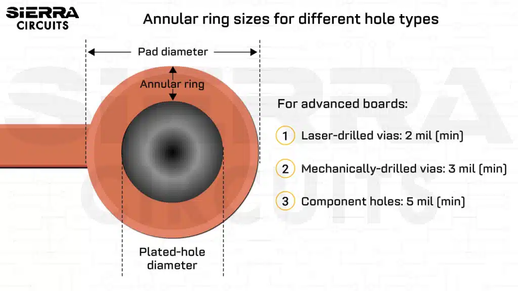
An annular ring provides reliable electrical connectivity and mechanical support around a PCB via. Even minor drill misalignment can lead to defects such as tangencies or breakout, compromising manufacturability and reliability.
Highlights:
- Have wider rings to reduce the probability of a breakout and improve reliability.
- Use teardrop pads to increase the structural integrity of traces less than 20 mil wide.
- Ensure the annular ring width meets or exceeds the manufacturer’s minimum requirements to prevent tangency or breakouts.
In this article, you’ll learn the importance of annular rings and how to calculate an accurate ring size to avoid common issues such as tangency and breakout.
What is an annular ring?
An annular ring is the copper area around a plated hole. It is essential for forming an electrical interface between a trace and a via.
How is an annular ring constructed?
When connecting traces to another layer in a multi-layered board, you typically have to place a copper pad on your circuit board and drill a via on it to make the connection. The outer ring surrounding the via after the PCB drilling process constitutes the annular ring.
Watch the full video to learn how to get the right annular ring.
Download the Design for Manufacturing Handbook to build cost-efficient PCBs without respins.

Design for Manufacturing Handbook
11 Chapters - 96 Pages - 90 Minute ReadWhat's Inside:
- Annular rings: avoid drill breakouts
- Vias: optimize your design
- Trace width and space: follow the best practices
- Solder mask and silkscreen: get the must-knows
Download Now
How do you calculate the annular size?
Annular ring width on a PCB is computed using the formula below:
(diameter of the pad – diameter of the finished hole) / 2
For example, if your pad diameter equals 22 mil and the hole diameter equals 10 mil, then the annular ring size is calculated in this manner: (22 – 10) / 2 = 6 mil.
Ideally, designers want their rings with holes located dead-center to get the best connection possible between the vias and the layers.
The size directly affects electrical reliability, mechanical strength, and manufacturability, acting as a safety margin that keeps vias and through-holes robust and functional.

The annular ring should be sufficiently wide to ensure a reliable electrical connection with the via. The minimum width of the ring should be greater than or equal to the specified width for the design. The table below provides minimum annular ring sizes for boards of different manufacturing classes.
| Manufacturing class | Mechanical drill (min annular ring) | Laser drill (min annular ring) |
|---|---|---|
| Standard | 4 mil | 3 mil |
| Advanced | 3 mil | 2 mil |
| Micro | 2 mil | 2 mil |
If the ring is too narrow than specified in the design, it can hinder component attachment and lead to pad breakout (zero annular ring), where the circuit overlaps or exits the pad or is eliminated due to drill misalignment. This reduces the circuit’s current-carrying capacity and compromises reliability.
To learn more, see our rigid PCB manufacturing capabilities.
What are the common annular ring issues?
The most typical annular ring defects include:
- Tangency: It occurs when the drilled hole is off-center, and its edge touches the edge of the copper pad. This means the hole is still within the pad but barely, reducing the effective annular ring width.
- Breakout: This happens when the drilled hole extends beyond the edge of the copper pad, eliminating part or all of the annular ring. This results in a weak or broken electrical connection and reduces the mechanical integrity of the via or pad.

Download our Design for Assembly Handbook to achieve error-free PCB assembly.

Design for Assembly Handbook
6 Chapters - 50 Pages - 70 Minute ReadWhat's Inside:
- Recommended layout for components
- Common PCB assembly defects
- Factors that impact the cost of the PCB assembly, including:
- Component packages
- Board assembly volumes
Download Now
How does the annular ring width affect the breakout probability?
The wider the annular ring, the lesser the breakout probability, as it provides a safety margin that absorbs drill misalignment without losing copper connection.

The via hole must be drilled at the absolute center of the pad to form the annular ring, or the minimum width of the ring must be above the specified value. Misregistration of the via concerning the land can lead to marginal interconnections that exhibit increased resistance and perhaps lead to reliability problems.
The graph below displays the probability of breakout plotted vs. the annular ring.

The smallest clearance (-1 mil) is intentionally designed to fail as a test to verify that the correct hole size was drilled. The probability of breakout decreases significantly, starting at 98% for a 2 mil clearance and dropping to 0% for clearances of 6 or 7 mil.
If the breakout is not acceptable, the supplier in this example would need to fabricate designs with annular rings of 6 mil or larger for the microvias. For 5 mil annular rings, the data indicates that 5% of the microvias will experience a breakout.

What is a teardrop pad?
A teardrop pad is an extra feature that adds additional copper at the junction of annular rings and PCB traces. It can increase the resilience against mechanical or thermal stress.

During the drilling process, there is a possibility of misalignment of the drill bit, which removes too much copper from the junctions of a via pad and PCB trace, causing the possibility of a broken trace connection or too thin a connection.
In such cases, a teardrop shape can increase the manufacturer’s tolerance of drilling in the pad, which can help reduce the rejection count in production.
The importance of using a teardrop increases as the traces become narrow. Teardrop rings are not necessary for conductors bigger than 20 mil. Also, teardrops are recommended for flex PCBs because of their structural integrity against shear and vibration.
An annular ring plays a critical role in PCB design and manufacturing. Hence, it’s a good practice to make sure all your annular rings are carefully crafted.
How can Sierra Circuits help you?
Sierra Circuits’ free Better DFM is an online tool that checks annular ring width, drill-to-copper clearance, hole registration, and other manufacturability rules to ensure your PCB meets reliable fabrication requirements.
When using this tool, you can go to “Advanced Options” and choose what you need to check for in your annular rings. You now have several options:
- Tangency is the default option. If you are willing to accept tangency on pads in your manufactured board, the Better DFM will look for a minimum of 5 mil (0.005″) annular ring width in your design.
- When you need to have a minimum 1 mil ring on pads in your manufactured board, then the Better DFM will look for a minimum of 6 mil (0.006″) annular width in your design.
- If you are targeting a ring of a minimum of 2 mil on pads in your manufactured board, the tool will look for a minimum of 7 mil (0.007″) ring width in your design.
- Lastly, if you do not mind having breakouts on pads in the manufactured board, the Better DFM will practically not look for any minimum ring width in your design. However, this option is not recommended.
The Better DFM does not only check for annular rings. The tool does a comprehensive design for manufacturability (DFM) analysis on your files.
The Better DFM tool’s 41-point checklist includes the following DFM checks:
| Category | Checklist items |
|---|---|
| Signal checks |
1. Conductor width
2. Spacing 3. Annular ring 4. Drill to copper 5. Hole registration 6. Text features 7. Missing copper 8. Features connection 9. Missing holes 10. Unconnected lines 11. Route to copper |
| Plane checks |
12. Drill to copper
13. Annular ring 14. Spacing 15. Conductor width 16. Thermal air gap / spoke width 17. Missing copper 18. Route to copper 19. Drill registration 20. Clearance smaller than the hole |
| Solder mask checks |
21. Solder mask clearance
22. Coverage 23. Route to mask 24. Spacing 25. Missing solder mask clearance 26. Exposed lines 27. Partial clearances |
| Silkscreen checks |
28. Silkscreen to mask spacing
29. Line width 30. Silkscreen to copper spacing 31. Silkscreen to hole spacing 32. Text height 33. Silkscreen to route spacing 34. Silkscreen over copper text |
| Drill checks |
35. Hole size
36. Duplicate holes 37. Hole spacing 38. Touching holes 39. Plane shorts 40. Holes to route 41. Missing holes |
Key takeaways:
- Ensure the copper pad around the drilled hole (via) is sufficient to establish a solid connection between copper traces and vias in multi-layer PCBs.
- Ensure the via hole is drilled in the center of the pad to prevent the copper from touching the edge of the pad.
- Incorporate tolerances in your design to account for potential mechanical or thermal stress during manufacturing and operation.
Well-designed annular rings ensure strong via connections, higher yields, and reliable PCB performance. By choosing the right ring width and validating it with DFM checks, you can avoid tangency, breakout, and costly respins.
Need assistance in designing your PCBs? Post your queries on our forum, SierraConnect, and have them answered by our experts.

About Rahul Shashikanth : Rahul Shashikanth is an electronics and communication engineer with over 8 years of experience in publishing technical articles on PCB design, manufacturing, and assembly. He is currently the content marketing manager at Sierra Circuits.


Start the discussion at sierraconnect.protoexpress.com