


Contents

On-demand webinar
How Good is My Shield? An Introduction to Transfer Impedance and Shielding Effectiveness
by Karen Burnham
An eye diagram is one of the most effective methods for analyzing the signal integrity of your PCB designs. It reveals the quality of high-speed signals by highlighting voltage levels and timing errors. As a PCB designer, you can use this eye pattern to diagnose issues that could lead to data errors.
In this article, you’ll learn how eye patterns are generated and how to analyze eye diagrams for signal integrity by evaluating the eye height, width, jitter, and amplitude.
Highlights:
- An eye diagram is a superimposed view of multiple digital signal cycles, forming an eye-like shape.
- It reveals critical signal integrity parameters such as bit error rate (BER), signal-to-noise ratio (SNR), and timing/voltage margins.
- A wide and tall eye indicates good signal quality, while a closed or skewed eye highlights problems such as jitter, crosstalk, and reflections.
- Eye diagrams are captured using real-time or sampling oscilloscopes and simulated using EDA tools (HyperLynx or Ansys SIwave).
What is an eye diagram in signal integrity analysis?
An eye diagram is a graphical representation of a digital signal over multiple cycles. It overlays thousands or millions of bit sequences on top of each other, resulting in an eye-shaped waveform.

Eye diagrams help you analyze signal integrity in your PCB design. They reveal how a signal varies over time relative to clock transitions. This depiction captures the cumulative effect of system anomalies such as jitter, noise, and inter-symbol interference.
Table 1: What eye diagram features reveal
| Eye feature | What it tells you |
|---|---|
| Wide eye | Good timing margin, low jitter |
| Tall eye | Good voltage margin, low noise |
| Closed eye | Severe jitter/noise, high likelihood of bit errors |
| Skewed crossing | Asymmetric signal rise/fall times |
| Multiple transition paths | Timing variations, possible crosstalk |
By examining the eye diagram in signal integrity analysis, you can evaluate key metrics such as bit error rate (BER) and signal-to-noise ratio (SNR). Comparing the measured eye pattern against predefined specifications or eye masks helps determine whether the signal meets design standards.
Eye diagrams are essential for testing and debugging high-speed PCB interfaces such as USB, HDMI, DisplayPort, and Ethernet. While eye patterns don’t convey protocol-level data, they are useful in diagnosing data-related electrical-level issues like bit errors, dropped packets, or receiver mismatches that can lead to system-level failures.
The infographic below demonstrates how eye patterns reveal signal integrity issues such as jitter, ringing, and inter-symbol interference. It also outlines effective strategies to mitigate these problems.

Equipment and simulation tools needed to generate an eye diagram
Eye diagrams can be created using physical test equipment or simulation tools, depending on the design stage and analysis needs.
- An oscilloscope is used to generate and display eye diagrams.
- Real-time oscilloscopes capture continuous, fast-changing signals and detect transient anomalies.
- Sampling oscilloscopes provide higher resolution and lower noise by reconstructing the signal over many cycles, but they can’t capture non-repetitive events. It must support a bandwidth of at least 1.5 to 2 times the signal frequency.
- A stable signal source is required to generate the digital signal for analysis. It can be a bit pattern generator, a function generator, or the actual transmitter in the system being tested.
- Bit error rate testers (BERTs) focus on evaluating the statistical error characteristics of the signal and help generate bathtub curves to evaluate jitter tolerance and eye-opening.
- Differential probes are essential to connect the oscilloscope to the signal source. They are commonly used to measure differential signals without introducing noise.
- The triggering mechanism allows the oscilloscope to capture data accurately by ensuring that signal sampling begins at the correct moment within each bit interval.
- A clock recovery unit is optionally used when the clock is not included with the data signal. It enables the oscilloscope to synchronize with the data signal.
Modern EDA platforms such as HyperLynx, Keysight ADS, or Ansys SIwave simulate eye diagrams for PCB design from channel models, predicting signal behavior before hardware fabrication.
To learn how S-parameters help you perform signal integrity analysis, see S-parameters measurement using a vector network analyzer.
How does an oscilloscope construct an eye diagram?
An oscilloscope captures multiple waveforms over time and layers them on top of each other to form an eye diagram.

On the left, different high-speed waveforms transmitted through the media are shown. An oscilloscope overlays these waveforms during each sampling period to form the eye diagram, capturing variations over several unit intervals (UI). A unit interval is the time between two consecutive transitions, also known as pulse time.
By recording numerous bit transitions, the eye pattern in signal integrity analysis reveals how electrical signals propagate through the transmission medium. To accurately reflect system performance, eye diagrams must be generated from many samples, often using pseudo-random bit sequences.
Many oscilloscopes allow you to define a “mask” around the ideal eye-opening. If the signal violates this mask, it indicates potential issues with jitter or noise.
Download our eBook to learn how to design high-speed PCBs with signal integrity.

High-Speed PCB Design Guide
8 Chapters - 115 Pages - 150 Minute Read
What's Inside:
Download Now
How to read and analyze an eye diagram?
The following characteristics serve as essential reference points for interpreting and analyzing the eye pattern in high-speed signal evaluation.
- Voltage levels (VH and VL): These elements of an eye diagram indicate whether the receiver will interpret the incoming signal as the correct logic level (VH for a ‘1‘ and VL for a ‘0‘). These levels are usually defined in the transmitter’s electrical specifications. If the signal stays within the expected voltage ranges, the system is more likely to interpret the bits accurately.

VH and VL represent the voltage thresholds used to determine digital logic levels in an eye pattern. - Leading and trailing edge: Bit transitions on the left and right sides of the eye diagram, respectively.
These bit transitions carry the high-frequency components of the signal. When analyzing the eye pattern, both the leading and trailing edges reveal how different equalization techniques and transmission media characteristics influence signal integrity.
- Crossover region: It highlights variations in bit transitions, commonly referred to as jitter. This region typically represents the widest part of the eye diagram. Analyzing this area is essential for understanding the impact of total system jitter.
- Eye-opening: The eye-opening is the most visually prominent feature, indicating the available timing and voltage margins for reliable data sampling.
- Eye height: It measures the vertical opening of the eye diagram, specifically the voltage difference between the lowest VH and highest VL. It reflects signal clarity; the greater the eye height, the better the signal-to-noise ratio.

Illustration showing the difference between eye amplitude and eye height. - Eye amplitude: This is the peak-to-peak voltage of a high-speed signal, defining the full swing between logical ‘1‘ and ‘0‘. It is firmly specified in standards for protocols like USB, PCIe, and FPD-Link. The one and zero levels used to calculate eye amplitude are typically measured around the 40%–60% range of the horizontal axis.
For clean signals, eye amplitude and eye height are similar. However, insertion loss often causes a noticeable drop in eye height.
- Eye width: It is the horizontal opening of the eye pattern and indicates the timing margin. Measured at the widest part of the eye, it shows how much time the signal stays valid and is critical for passing eye diagram compliance tests.
- Edge rate: It is the speed at which a signal transitions between its high and low voltage levels. It is typically measured between the 90% and 10% voltage levels of a signal transition. However, depending on the specification, it may also be measured using alternative thresholds such as 80% to 20% or 70% to 30%.
- Eye mask: This is a predefined keep-out region in the eye diagram, defined by six key points that specify the minimum eye opening and acceptable voltage limits. Any signal sample falling inside this region is considered an eye mask violation.

A signal should not enter the eye mask region to ensure reliable data transmission.
Passing an eye diagram test requires zero eye mask violations, which is essential for compliance with high-speed data protocols. Signal conditioners may be needed to meet these requirements and ensure reliable performance.

- Eye-crossing percentage: It calculates the amplitude at the crossing point of rising and falling edges in the eye diagram. It reflects duty cycle distortion and signal symmetry, helping assess the timing balance between logical ‘1‘ and ‘0‘.
To calculate the crossing percentage, apply the following formula:
Eye crossing % = 100 ✖ [(crossing level – zero level)/(one level – zero level)]
Where,
-
- Crossing level: The voltage where the rising and falling edges intersect.
- One level: Average voltage for logic high (‘1‘).
- Zero level: Average voltage for logic low (‘0‘).

- Noise margin: Vertical noise shifts indicate power supply variations and electromagnetic interference (EMI), both of which can compromise data integrity. A smaller eye height indicates a reduced noise margin, which can lead to data errors.
- Bit error rate (BER): Evaluates the probability of signal errors due to poor signal integrity. While not a direct visual feature of the eye diagram, BER is strongly correlated with eye closure (the lower the eye height, the higher the BER).
- Bit period: Corresponds to the horizontal width of the eye, including the crossing points. It is used as a time reference to measure jitter, eye width, and sampling position.

The bit period is indicated by the horizontal opening of an eye diagram in signal integrity analysis. - Rise and fall time: These define the speed of a signal’s transitions between voltage levels. Rise time measures the transition from low to high (typically from 10% to 90% of the peak amplitude), while fall time measures the transition from high to low (90% to 10%). Slow transitions can blur the eye contour and reduce signal clarity.

High-speed signals rise sharply, and low-speed signals transition gradually. - Overshoot: This occurs when the signal exceeds its intended voltage level during a transition. It appears as the first peak or dip, typically appearing as a sharp pulse. Excessive overshoot can stress or damage circuit components. It may trigger the protection diode, potentially leading to early failure.

Illustration showing how signal overshoot and undershoot appear as peaks or dips in an eye diagram.
- Undershoot: This happens when the signal dips below its expected minimum level after a transition. It refers to the subsequent peak or valley value. A significant undershoot can lead to false clock signals or data errors.
- Threshold/crossing percentage: The lowest signal level a receiver can detect while maintaining an acceptable bit error rate, especially under degraded transmission conditions.

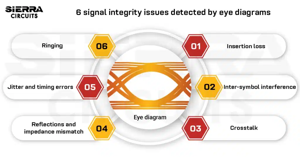
6 signal integrity issues revealed by eye diagrams
High-speed signals must maintain their quality as they travel through the transmission medium and any components along the path. Poor signal integrity can lead to incorrect data interpretation at the receiver, resulting in link failure.
Eye patterns provide a visual snapshot of signal quality over time. By analyzing the shape and clarity of the eye pattern, signal-integrity engineers can identify underlying issues that impact performance.

Here are some common problems that eye diagrams can help identify.
| Signal integrity issues | Description | Impact on the eye diagram |
|---|---|---|
| Insertion loss | Frequency-dependent attenuation of signal power as it travels through the transmission channel. Longer traces cause more high-frequency loss. |
|
| Inter-symbol interference (ISI) | Signal overlap due to limited bandwidth or lossy traces, causing energy leakage between bits and time/frequency domain overlap. |
|
| Crosstalk | Noise induced by adjacent signal traces through electromagnetic interference. |
|
| Reflections and impedance mismatch | Abrupt discontinuities cause signal bounces due to impedance mismatches. |
|
| Jitter and timing errors | Timing deviations from ideal signal edge positions due to clock instability, noise, or interference. |
|
| Ringing | Oscillations after rapid voltage changes due to underdamped transitions. |
|
The simulation images below compare eye diagrams with and without ringing effects in PCBs.

At Sierra Circuits, we can build PCBs with ±5% impedance tolerance. We add impedance test coupons to each panel and validate the impedance to ensure it matches your requirements. These test coupons replicate the trace structure and layer stack-up of the actual PCB.

See our controlled impedance capabilities to learn more.
Signal conditioning techniques to improve the eye diagram
These techniques are typically implemented within integrated circuits (ICs) and are essential for maintaining performance in high-speed data transmission systems.
1. Receiver equalization: selectively amplifying high-frequency signals
This technique compensates for frequency-dependent losses introduced by transmission media. Positioned at the receiving end, it selectively amplifies high-frequency components that tend to degrade during transmission.
How it works:
Equalization applies a high-pass filter whose response ideally mirrors the inverse of the channel’s loss profile. This helps flatten the signal’s frequency response, restoring amplitude and reducing distortion and inter-symbol interference (ISI).

Key considerations:
- Equalizers must offer enough bandwidth to restore signal quality at the highest frequencies.
- They are often programmable or adaptive, allowing them to adjust automatically to different channel conditions and media types.
- Excessive equalization can lead to over-equalization, causing new forms of distortion.
If the equalization is too aggressive, it can lead to over-equalization, where high-frequency signals are disproportionately amplified.

This can introduce distortion in the eye diagram, such as:
- Double banding: Parallel lines along the rising or falling edges, where symbol transitions are unevenly emphasized.
- Reduced eye width: Increased jitter and noise at lower frequencies.
- Increased eye height: Can mislead and suggest signal improvement despite underlying instability.
To avoid these pitfalls, equalization parameters must be carefully tuned to match the transmission channel characteristics, ensuring optimal compensation without distortion.
![]()
2. Pre-emphasis: boosting high-frequency at the transmitter
Pre-emphasis is a signal conditioning method applied at the transmitter end. It works by boosting the selective high-frequency components of a signal. To mitigate inter-symbol interference, it enhances the energy of the signal’s high-frequency components, primarily the edges, relative to the low-frequency, steady-state portions of the waveform.

How it works:
It pre-compensates for high-frequency losses by boosting signal transitions above the typical logic-high (VH) level or below the logic-low (VL) level, enhancing edge sharpness. Ideally, the transmission medium cancels out the boost by the time the signal reaches the receiver, allowing it to interpret a standard logic ‘1‘ or ‘0‘.

In the eye diagram, pre-emphasis introduces variation in the signal transitions:
- Edges may appear steeper or overshoot VH/VL levels.
- Faster rise time in the leading edges indicates the presence of pre-emphasis.
- Crossover points remain mostly unaffected, preserving timing accuracy.
Excessive pre-emphasis, however, can cause distortion in the eye diagram, particularly in high-speed serial communication links.

It can lead to:
- Double banding.
- DC violation (e.g., IMS DC high/low thresholds).
- Signal distortion, particularly if the boost exceeds what the channel can appropriately attenuate.
Pre-emphasis works to boost the high-frequency content of the data by boosting the edge transition of the signal above the actual VH level or below the VL level. Ideally, the boost would be canceled out perfectly by the transmission media right at the receiver. So, the data receiver sees a regular bit ‘1′ or bit ‘0′.
This technique helps compensate for transmission losses and ensures that signals arrive at the receiver with minimal distortion, essential for noise-free RF PCBs.
At Sierra Circuits, we fabricate high-quality RF PCBs with tightly controlled curing parameters such as temperature, pressure, and time to minimize stress and prevent layer misalignment.
Visit our RF and microwave PCB capabilities to learn more.
3. De-emphasis: attenuating low-frequency signals at the transmitter
De-emphasis is the counterpart to pre-emphasis and is also applied at the transmit end. Instead of amplifying high-frequency signals, it attenuates selective low-frequency components, particularly the flat, steady-state portions of the waveform.
How it works:
This selective attenuation improves the relative prominence of signal transitions by reducing the DC level of long-duration symbols (multi-bit logic highs or lows). The effect is an improvement in the signal-to-noise ratio and better preservation of edge clarity at the receiver.

As with pre-emphasis, identifying de-emphasis in an eye diagram can be tricky.

It can be identified by:
- Reduced amplitude in flat segments between transitions.
- Edge transitions that may fall below VH or rise above VL.
- Minimal impact on jitter and crossover regions, much like pre-emphasis.
As with other techniques, excessive de-emphasis can lead to the collapse of the amplitude of repeated bits and increasing susceptibility to bit errors.

It can cause:
- Double banding and increased variability in signal levels.
- Distorted signal shapes that may reduce eye height and clarity.
Each of these signal conditioning techniques is critical to maintaining signal integrity in high-speed digital systems. However, overuse or improper tuning can introduce new sources of distortion. Precise parameter optimization tailored to the specific transmission line characteristics is essential.
Download our eBook to learn how to design reliable RF and microwave PCBs.

RF & Microwave Design Guide
8 Chapters - 44 Pages - 60 Minute Read
What's Inside:
Download Now
7 best practices for eye diagram analysis in high-speed data links
- Place the oscilloscope as close as possible to the transmitter for a high-speed data link to minimize the influence of cabling and PCB traces. This setup ensures you are measuring the transmitter’s true performance under ideal conditions, free from external effects.
- Ensure the oscilloscope has sufficient bandwidth to capture the signal’s transitions accurately.
- Verify key electrical parameters using an eye diagram, including VH, VL, peak-to-peak voltage, pre-emphasis or de-emphasis, edge rates, and deterministic jitter from the transmitter. Confirm that the transmitter behaves as expected and determine the need for signal conditioning.
- Place the signal source close to the receiver to minimize additional losses from transmission media and probe loading. Account for unavoidable losses in your eye diagram analysis, as these can impact receiver evaluation.
High-speed receivers sample at the most open part of the eye pattern, known as the optimal sampling region.

-
- Sampling within this region maximizes signal integrity and minimizes bit errors, as it avoids interference from adjacent bits.
- Sampling outside this window increases the risk of data corruption. This optimal region typically aligns with the eye mask used during eye diagram testing.
- Evaluate receiver performance for a given input by testing equalization schemes, internal termination loading effects, noise immunity, and jitter tolerance. Use eye diagrams to understand how the receiver interacts with specific input signals during system design.
- Consider the influence of transmission media, signal path components (such as ESD devices), and external noise sources on the interaction between the transmitter and receiver when measuring eye diagrams from a system-level perspective.
- Measure signals at multiple points in the system to aid in debugging. Use eye patterns to identify issues such as receiver equalization, transmit pre-/de-emphasis, inter-symbol interference, and impedance-induced reflections that impact system-level performance.
Key takeaways:
- Eye diagrams help detect signal integrity issues like insertion loss, ISI, crosstalk, ringing, jitter, and impedance mismatches, each distorting the eye pattern in distinct ways.
- The size of the eye-opening directly reflects the timing and voltage margins—larger openings mean better chances for accurate data sampling.
- Variations in the crossover point of the eye diagram in signal integrity analysis provide insight into total system jitter and timing uncertainties.
- Fast edge rates (rise/fall times) contribute to sharper transitions in the eye, which is critical for clear signal definition at high data rates.
- The horizontal scale of an eye diagram is based on the bit period, which helps define sampling positions and quantify jitter.
- Eye masks define a no-go zone within the eye; any signal sample that intrudes into this mask is flagged as a violation and potential compliance failure.
- Receiver equalization, pre-emphasis, and de-emphasis are used to restore or improve signal quality. Each method modifies the waveform to combat transmission losses.
- Excessive signal conditioning (over-equalization or over-emphasis) can introduce new distortions, such as double banding or eye height misrepresentation.
- Proper oscilloscope placement, bandwidth matching, and testing at both transmitter and receiver ends ensure accurate and meaningful eye diagram results.
The eye diagram remains one of the most potent diagnostic tools in digital signal integrity analysis. Its graphical power, married with precise metrics, bridges the gap between abstract theory and tangible design insight. For engineers navigating the labyrinth of high-speed design, mastering the eye diagram is not optional—it’s fundamental.
Have questions about your high-speed printed board design? Post your queries on SierraConnect. Our PCB experts will answer them.

About Pooja Mitra : Pooja Mitra is an electronics and communication engineer. With an experience of over three years in the PCB industry, she creates industry-focused articles that help electrical and PCB layout engineers.


Start the discussion at sierraconnect.protoexpress.com