


Contents
An efficient PCB power supply design ensures stable voltage delivery and reliable current distribution across all circuit components. A poorly designed power supply can introduce voltage fluctuations, overheating, and signal integrity issues.
To ensure consistent performance, circuit board engineers must carefully select regulators, optimize thermal performance, and implement efficient grounding and decoupling practices.
In this article, you will learn 7 important PCB power supply design considerations that can help improve power integrity and thermal performance.
Highlights:
- Use low-dropout (LDO) regulators to reduce power loss and improve heat dissipation in low-voltage circuits.
- Implement heat sinks, thermal vias, and forced-air cooling to prevent hotspots.
- Isolate noisy digital power supplies from sensitive analog circuits to minimize noise coupling.
- Place 0.1 μF decoupling capacitors close to IC power pins to suppress voltage fluctuations and switching noise.
Why is PCB power supply design important?
PCB power supply design is critical for maintaining stable and reliable operation of all circuit components. It not only converts AC power to DC power but also ensures clean and consistent power delivery throughout the board.
Modern electronic devices often operate at low voltages such as 1.8V and 1.2V, making them highly sensitive to voltage ripple, noise, and transient fluctuations. Poor power supply design can lead to signal integrity issues, overheating, EMI, unstable operation, and reduced system reliability.
An efficient PCB power supply design helps minimize power loss, reduce heat dissipation, improve power integrity, and ensure that every component receives clean and stable power under varying load conditions.
Power supplies also require current limits to limit the maximum current. Thus, the important parameters for a power supply are voltage, max current, voltage ripple, and heat loss at maximum current.

The typical power flow of an electronic circuit for a power supply is shown in the above figure. Electronic circuits need voltages from 1.8 V to 12 V. 1.2 V, 1.8 V, 3.3 V, 5 V, and 12 V are the most common voltages used.
In the first stage, input AC voltage at 230 VAC/110 VAC is converted to an isolated DC voltage in the range of 6-12 V. A buck-switching regulator is employed in the second stage, which converts the 6-12 V to 5 V or 3.3 V. Further, the 3.3 V is converted to 1.8 V or 1.2 V using low-dropout regulators.
Before the advent of Switched-Mode Power Supplies (SMPS – switching power supplies), iron core transformers were used to convert high voltages, 230 VAC/110 VAC, to 12 VAC. This was further rectified by diode bridge rectifiers to DC volts approximately 12 x 1.4 = 16.8 VDC maximum. Linear regulators were used to reduce the voltages to the required levels.
The disadvantages of such circuits were poor power efficiency (less than 80%), high heat loss, a larger PCB footprint, and poor power ripple. The use of switching power supplies has improved the efficiency of converting voltages to lower levels, reduced the footprint of power supplies (very small and light in size), and reduced ripple.
A larger amount of power was previously lost in linear regulators due to higher dropout voltages. For example, consider the linear voltage regulator LM7805. LM7805 (5 V) typically has a dropout voltage of approximately 7.5 V, requiring a minimum of approximately 2.5V difference between input and output voltage. Therefore, for a 1A regulator, the power loss at 7.5 V input will be 2.5 V x 1A = 2.5 W.
With the low dropout regulator LM1117-5.0, the dropout voltage is 6.2 V, requiring an input voltage of Vout +1.2 V at the input. A combination of switching regulators and LDO is used to increase efficiency for critical applications. For example, from stage one, if 7.5 volts is available, this will be dropped to 3.3 V with a buck converter and then dropped to 1.8 V using a linear regulator LM1117-1.8.
See 4 common PDN design challenges and how to resolve them to learn about power distribution network design.
7 tips for designing a stable PCB power supply
1. Choose between linear and switching regulators

Generally, designers have two options in choosing power supply regulators: linear regulators and switched-mode regulators. The linear regulators provide low noise output but have higher heat dissipation, which requires cooling systems. The switched-mode regulators are highly efficient over a broad current range, but the switching noise causes spikes in response.
A linear-mode regulator requires an input voltage higher than the required output voltage because there will be a minimum voltage dropout. Linear regulators have considerable power loss and heat dissipation, which makes them less efficient.
If you are considering a linear regulator for your PCB design, then you must consider a regulator with low voltage dropout, and the thermal analysis must be done before going to fabrication. Besides that, linear-mode regulators are simple, cheap, and provide exceptionally noiseless voltage outputs.
The switching regulators convert one voltage to another by temporarily storing energy in inductors and then releasing that energy at a different voltage at different switching times. In such power supplies, fast switching MOSFETs are used. The output from these highly efficient regulators could be adjusted by altering the duty cycle of the Pulse Width Modulation (PWM). The efficiency depends on the heat dissipation of the circuit, which is low in this case.
The PWM switching of switching regulators causes noise or ripple in the output. Switching currents can cause noise crosstalk in other signals. Thus, switching power supplies need to be isolated from critical signals.
Switched-mode regulators use MOSFET technology, so it is obvious that they emit EMI (Electromagnetic Interference) noise. We cannot eliminate EMI from any circuit completely, but we can minimize it by EMI-reducing measures like filtering, reducing current loops, ground planes, and shielding. Electromagnetic Compatibility (EMC) measures should be considered before incorporating switched-mode regulators in your design.
When it comes to choosing a voltage regulator, linear and switching-regulated power supplies are the two obvious choices. A linear-controlled power supply is cheaper but inefficient and dissipates more heat. Meanwhile, a switching-regulated power supply is more expensive and requires the connection of more passive components, but it doesn’t easily heat up.
Sierra Circuits fabricates and assembles high-quality circuit boards in the United States. Visit our PCB manufacturing capabilities to learn more.
2. Place decoupling and bypass capacitors near IC power pins

When power is distributed to the components across the board, different active components will cause ground bounce and ringing in a power rail. This could lead to voltage drops near the power pins of components. Under these circumstances, designers use decoupling and bypass capacitors near the power pins of components to provide for short spikes in the current requirement of the device.
The concept behind decoupling is to reduce the impedance between power and ground. The decoupling capacitors act as a secondary power source, providing the current the IC needs, and as a local charge source to support a switching event.
The bypass capacitors bypass the noise and reduce fluctuation in the power bus. They are placed closer to the devices or ICs and linked between power and ground to compensate for changes in the power and ground plane potential when many ICs switch simultaneously.
The bypass capacitors are used to suppress inter-system or intra-system noise within an electrical network. All decoupling capacitors have to connect close to the IC’s power pins and the other end directly to a low-impedance ground plane. Short traces to the decoupling capacitors and ground vias are required to minimize additional inductance in series for this connection.
Several aspects must be considered when selecting a local bypass capacitor. These factors include selecting the correct capacitor value, dielectric material, geometry, and capacitor location relative to the IC. The typical value of the decoupling capacitors is 0.1 μF ceramic.
For more layout strategies, download the high-speed design guide.

High-Speed PCB Design Guide
8 Chapters - 115 Pages - 150 Minute ReadWhat's Inside:
- Explanations of signal integrity issues
- Understanding transmission lines and controlled impedance
- Selection process of high-speed PCB materials
- High-speed layout guidelines
Download Now
3. Implement relevant thermal management techniques

The performance of a power supply directly depends on the heat dissipation. Most electronic components emit heat whenever current passes through them. The amount of heat emitted depends on the component’s power level, characteristics, and impedance. As mentioned earlier, choosing a suitable regulator can reduce heat dissipation in a circuit. The switched regulators are highly efficient since they dissipate less heat.
Electronic circuits operate more effectively at lower temperatures. Designers should consider proper cooling methods to ensure devices work at ambient temperature.
If the designer chooses a linear regulator, a heat sink, or other cooling methods are recommended if the system allows it. Fans can be incorporated into the design to ensure forced cooling if a device has high heat dissipation.
Heat dissipation throughout the PCB may not be even. Components with high power ratings may dissipate a considerable amount of heat, creating a hotspot around them. Thermal vias can be used near these components to transport heat away from the region quickly.
Combining heat-dissipating techniques and cooling methods can create a highly efficient power supply design. Designers can use either conduction cooling methods, such as the heatsink, heat pipes, thermal vias, or convection cooling methods, like cooling fans, thermoelectric coolers, etc.
For more, see 12 PCB thermal management techniques to reduce heating.
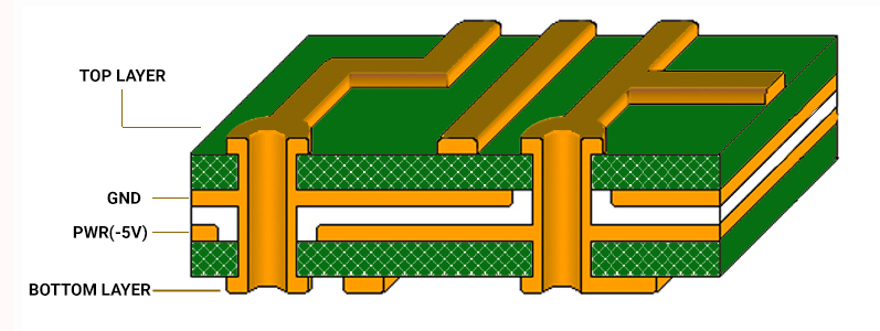
4. Use dedicated ground and power planes

Ground planes and power planes are low-impedance paths for power transmission. A power supply needs separate ground planes to distribute power, reduce EMI, minimize crosstalk, and reduce voltage drops. The power planes are dedicated to transmitting power to the required areas of the PCB.
You need to treat sections of the ground network separately. In a multilayer board, one or more layers can be dedicated specifically to ground and power planes. They can also reduce interference and crosstalk by placing ground planes between two active signal layers, thereby effectively surrounding the signal traces with the ground.

5. Utilize EMI filters to reduce conducted and radiated noise
EMI radiation can occur from any power lead entering or leaving a power supply’s enclosure. The PCB designers expect the power supply to keep its EMI levels below the frequency spectrum limit they define. Therefore, EMI filters are used at power input points to reduce conducted noise.
For more on EMI, read 7 tips and PCB design guidelines for EMI and EMC
An EMI filter’s architecture allows it to block high-frequency noise. It is critical that the designer carefully lay out the filter circuit components to prevent the components from transferring energy into the traces that connect them
For more, download the EMI and EMC Design Guidelines for PCBs.
EMI and EMC Design Guidelines for PCBs
6 Chapters - 77 Pages - 75 Minute ReadWhat's Inside:
- How electromagnetic interference is generated and spreads
- How to identify EMC requirements and applicable standards
- How to design for electromagnetic resilience
- Common EMI sources: Switching circuits, PWM signals, and motors
- PCB structures that cause radiated emissions
- Practical layout, stack-up, filtering, and shielding guidelines
Download Now
6. Position output capacitors near regulators to prevent voltage overshoot
When power supplies are loaded suddenly, say from no load to full load, the voltage output will tend to dip briefly and return to normal voltage.
In some cases, the output will oscillate for some time before the voltage settles to normal. If the oscillations are beyond the design limits, it will be necessary to tune the output and compensation capacitors. For example, for LM7805, it’s recommended to put a 0.1μF capacitor next to the output pin. Similarly, sudden unloading of the regulator could cause overshoot and oscillations.
Make sure that the components selected are within design constraints for a better response from circuit design. Whether the circuits are AC or DC, they have different responses. AC and DC circuits should be considered separately.
Need help designing a stable PCB power supply? Our engineering team can help you optimize thermal management and EMI performance to improve power integrity and ensure reliable board operation before you finalize your design.
You can book a meeting with our experts or call us at +1 (800) 763-7503.

7. Perform simulations to identify hotspots
Designers should ensure the power integrity of the power supply design. It is simply the quality of power delivered to the circuit.
Power integrity is the measurement of how effectively the power is transferred from the source to the load within a system, which ensures all the circuits and devices are supplied with the appropriate power to achieve the desired performance of the circuit.
A power supply with less noise can ensure higher power integrity. Design for power integrity is nothing but managing the power supply noise.
There are simulation tools that help to estimate the power quality in a circuit. Such tools help estimate voltage drops, recommend placement of decoupling capacitors, and also identify hotspots of high current flow in the circuits.
To learn about circuit simulation, read how does circuit simulation work?
Good power supplies are the key to an electronic device’s accurate functioning. As we have seen, the PCB designer has several options available when considering a power supply design. The choice of regulators, capacitors, and EMI filtering is important in those considerations. Similarly, the thermal effect and load response should be considered while designing a power supply system.
At the same time, follow the recommendations mentioned in the power supply IC datasheets. The trace thickness and component placement are critical in the power supply design.
If you need any assistance in power supply design, please post your question on our circuit board forum, SierraConnect. Our PCB experts will answer them.


