


Contents

On-demand webinar
How Good is My Shield? An Introduction to Transfer Impedance and Shielding Effectiveness
by Karen Burnham
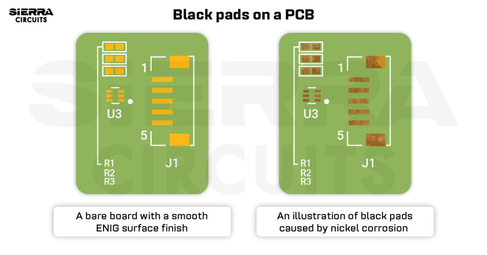
Black pad is a surface finish defect associated with electroless nickel immersion gold (ENIG) in PCBs, caused by excessive corrosion of the nickel layer. It often goes undetected during standard QC procedures, as the gold layer masks the underlying nickel.
To minimize this risk, fabricators tightly control the nickel-phosphorus stoichiometry and immersion gold bath chemistry. This prevents aggressive corrosion that can compromise solder joint reliability.
Highlights:
- Black pad is a localized corrosion of the electroless nickel layer occurring during the immersion gold process.
- Excessive phosphorus accumulation at the nickel boundaries is a primary driver of the defect.
- Since gold covers the corrosion, the issue often remains invisible until mechanical stress causes solder joint failure.
- IPC-4552 governs the thickness and quality requirements for ENIG to minimize these risks.
- Success relies on strict control of bath chemistry, pH levels, and immersion timing.
In this article, you will learn the root causes of black pad, the chemical reactions behind nickel corrosion, and the IPC standards required to ensure solder joint reliability.
What does black pad mean?
A black pad is a surface finish flaw that occurs due to corrosion and oxidation of the electroless nickel. It primarily begins at the nickel grain boundaries and then spreads as the corrosion increases. As the deposited gold thickness increases, the oxidation of nickel may increase.
This defect reduces solderability and leads to weak solder joints. When those joints come under pressure, they break easily and leave exposed corroded nickel behind, hence the name black pad.
ENIG became popular because of several advantages. They include:
- Good shelf life
- Easy inspection
- Nickel layer protects plated through-holes during testing

The surface finish gained wider adoption with the shift toward lead-free manufacturing and RoHS compliance. Although fabricators have improved process control to mitigate black pad, it remains a critical reliability concern that designers and manufacturers must address.
What causes a black pad?
Black pad is primarily caused by high phosphorus content in the nickel layer and aggressive immersion gold chemistry. These factors degrade the nickel surface, resulting in weak solder joints and reliability issues.
The key contributors are explained below:
1. High phosphorus content
Reflow cycles and rework during the ENIG process can increase the phosphorus concentration in the nickel layer, ultimately weakening it. As nickel dissolves, phosphorus remains behind, creating a brittle, phosphorus-rich surface. Higher phosphorus content is strongly associated with black pad formation.
2. Corrosion during gold deposition
During ENIG, gold deposition occurs through a controlled corrosion reaction on the nickel surface. However, aggressive gold bath chemistry or excessive gold thickness can accelerate this reaction, leading to black pad.
It is generally accepted to keep the gold thickness to 2-4 μin, as per the IPC-4552 ENIG specification.
For more, read what is conformal coating.
3. Brittle fracture
In some cases, what is identified as a black pad is actually a brittle fracture, as both produce a cracked nickel structure after gold removal. This fracture occurs when tin dissolves a part of the nickel, leaving behind a thin, phosphorus-rich layer that does not dissolve. Thermal stress, vibration, or mechanical shock can then weaken the metallurgical bonds, leading to a black pad.
What are the practical solutions to black pad?
Black pad can be minimized through tight process control of the ENIG line, particularly the nickel bath, immersion gold chemistry, and pretreatment steps. Fabricators achieve this by maintaining proper bath chemistry, controlling phosphorus content, and ensuring consistent surface preparation.
Each of these process controls is discussed below:
- A well-controlled nickel bath is one of the ways to the elimination of this defect. For that, it is essential to verify any potential ENIG provider’s baths and processes. Many requirements have to be met across the ENIG line to minimize the risk of black pad, including pretreatment (removing oils and other residues to prepare for PCB etching) and the use of chelating agents as well as stabilizers to prevent the nickel in the bath from plating out into the tanks.
- Generally, it is found after the PCB manufacturing process when the board is already populated. To identify the presence of black pad, it is required to look for certain flaws (cracked structure, non-planar surface, etc.) and to consider alternative finishes accordingly.
- It may be possible to rule out black pad after inspecting the surface of a finished board. For example, if there are no spikes and dark bands near the nickel boundaries, then it may not be an issue.
- Controlling the gold bath by maintaining the stoichiometry of nickel and gold can resist the black pad. It is also important to keep tabs on the pH level to know how much phosphorus will ultimately be plated.

What are the performance specifications for ENIG?
In 2002, IPC issued a specification (IPC-4552) for ENIG. During that time, tin-lead solder was predominant in PCB assembly, and lead-free soldering was not a widely established concept.
According to IPC-4552,
- Electroless nickel thickness- 3 to 6 μm [118.1 to 236.2 μin]
- Immersion gold thickness- 0.075 to 0.125 μm [2.955 to 4.925 μin]
The specification was amended in 2012 due to the rising price of gold. The lower limit for gold thickness was decreased from 0.05 μm to 0.04 μm (1.6 μin).
At Sierra Circuits, we adhere to IPC specifications unless the customer specifies otherwise. The thickness of the coating can be measured using an XRF (X-ray fluorescence spectroscopy) technique.
To learn more about PCB assembly and testing, download the Design for Assembly Handbook.

PCB Design for Assembly Handbook
6 Chapters - 50 Pages - 70 Minute ReadWhat's Inside:
- Recommended layout for components
- Common PCB assembly defects
- Factors that impact the cost of the PCB assembly, including:
- Component packages
- Board assembly volumes
Download Now
A glance at IPC-4552 revisions
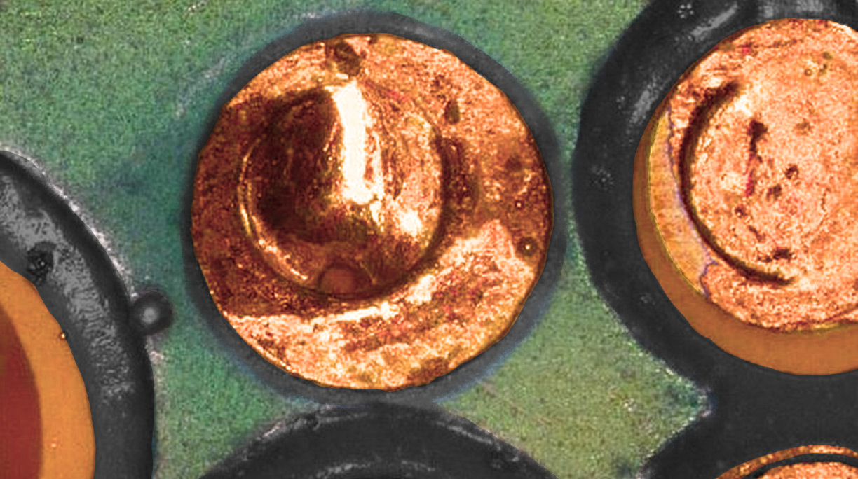
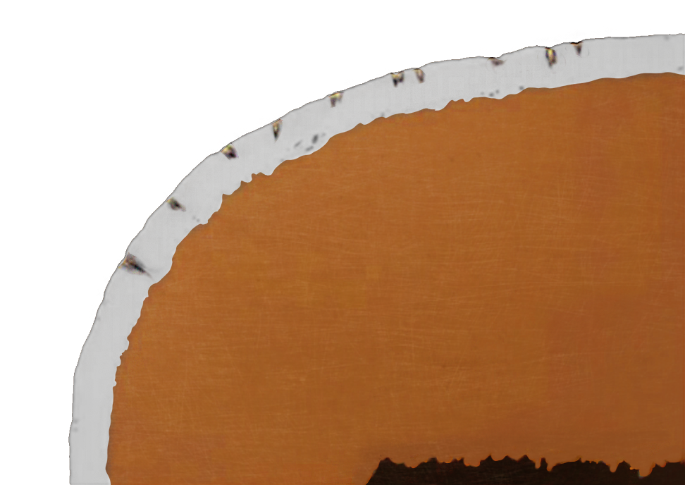
IPC-4552 revision A, released in August 2017, describes nickel corrosion defects as spikes, spreader spikes, and black bands, visible in cross-sectional analysis at 1000× magnification. It also categorized them into severity levels based on depth and occurrence.
| Corrosion level | Description | Disposition |
|---|---|---|
| Level 1 | <10 defects with <20% depth penetration | Acceptable |
| Level 2 | Defects more than Level 1 and less than Level 3 | Requires resolution |
| Level 3 | >10 defects with >20% depth penetration | Rejectable |
Revision A is concerned with the electroless nickel layer’s resistance to corrosion due to poorly controlled electroless nickel plating processes during the immersion gold stage. It is crucial to focus on the chemical reactions of how the gold plating is done to understand nickel corrosion caused by immersion gold plating.
Anodic reaction
Ni → Ni2+ + 2e–
Cathodic reaction
2[Au(CN)2] – → 2Au+ + 4CN–
2Au+ + 2 e– → 2 Au
Overall reaction
Ni + 2[Au(CN)2] – → 2Au + [Ni(CN)4] 2
The gold is deposited onto the nickel surface through an exchange reaction (displacement of Ni by Au atoms), also known as an immersion reaction. This reaction is determined by electron transfer and controlled by an electromotive series (an arrangement of elements and ions), stating that more noble metals will naturally plate onto less noble ones without any chemical reducing agents.
It is necessary to transfer electrons from the metallic electroless nickel deposit to the gold ions in solution to deposit gold on the electroless nickel surface. As the reaction proceeds, this electron transfer causes metallic nickel (corrosion) to be removed from the surface and builds up nickel ions in the immersion gold solution.
There will always be some level of corrosion in gold plating since nickel needs to be removed from the surface of the electroless nickel deposit to facilitate the gold metal deposition.
EPIG surface finish is one of the newer technologies, introduced as an alternative to electroless nickel immersion gold (ENIG). Unlike ENIG, it eliminates the use of nickel, avoiding nickel corrosion issues.
Revision A defined the defect and how to evaluate it. However, this meant that even a single level 3 defect could reject an entire lot, which wasn’t practical for real-world manufacturing. IPC-4552 revision B, released in April 2021, addresses this by introducing product rating. The standard evaluates the occurrence of corrosion across multiple inspection locations. It gives a more realistic picture of reliability and solderability risk.
Instead of evaluating a single microsection, this update:
- Recommends a specific method to strip the gold.
- Identifies the most affected areas at low magnification (200X).
- Performs detailed classification at 1000X.
- Tabulates results into a product rating (0 – 3) based on defect distribution (as shown below).
| Product rating | Corrosion investigation | Disposition |
|---|---|---|
| 0 | Defect-free, zero evidence of corrosion | Acceptable |
| 1 | >60% of evaluated locations show level 0 or level 1 | Acceptable: this level of corrosion will not degrade solder joint integrity |
| 2 | Corrosion defects and frequency > product rating 1 but < product rating 3 | Acceptable: provided that solderability meets requirements per section 3.9 |
| 3 | >40% of evaluated locations show level 3 defects | Nonconforming: This level of corrosion will degrade solder joint reliability |
Another important addition in rev B is the requirement to measure phosphorus content in the electroless nickel (EN) layer using energy dispersive X-ray fluorescence (EDXRF). Phosphorus percentage is a key indicator of EN bath condition and stability. It also correlates with increased susceptibility to nickel corrosion.
This measurement helps fabricators to track bath aging (through metal turnovers) and proactively adjust process parameters. It ensures that ENIG-related risks, particularly black pad-induced solder failures, are controlled at the process level rather than detected after assembly.
To learn how to avoid DFM issues, download the Design for Manufacturability Handbook.

Design for Manufacturing Handbook
11 Chapters - 96 Pages - 90 Minute Read
What's Inside:
Download Now
What is hyper-corrosion of nickel?
Hyper-corrosion of nickel in ENIG is an abnormal, aggressive chemical attack on the nickel layer during plating, leading to surface defects and compromised solderability.
Black-pad defects are formed by the hyper-corrosion activity of the immersion gold process on the nickel surface. Gold and nickel atoms undergo galvanic hyper-corrosion, resulting in depletion of nickel and enrichment of phosphorus atoms in the localized area.
Black pad, caused by a poorly formed joint at the solder/nickel-phosphorus interface, can lead to failures and de-wetting of the solder. Hyper-corrosion involves the prevention of intermetallic formation and wetting of the surface (solder). This causes de-wetting, a solid-to-liquid bond failure, and interfacial fracture of the solder.
As per IPC-4552A, the average gold thickness should be three standard deviations above 1.58 μin and three standard deviations below 3.94 μin.
The gold thickness should have an average of
-3 s ≥ 1.58 μin, and
+3 s ≤ 3.94 μin
Where, = variable and s = standard deviation.
PCB manufacturers must comply with this thickness limit to maintain a high level of quality and reliability. The achievement of a lower limit of thickness and tight uniformity control improves the reliability of boards and reduces costs significantly.
Here are a few important points to consider from a manufacturer’s perspective:
- It is always possible to find hyper-corrosion if sufficient samples are taken from a circuit board or if excessive magnification is used for inspection. However, a single instant of hyper-corrosion is acceptable.
- In hyper-corrosion, a non-wetting defect occurs (despite the gold being consumed) as a result of the lack of intermetallic compound (IMC) formation.
- Hyper-corrosion is acceptable if it does not interfere with the formation of a reliable solder joint, as defined by continuous IMC formation.
- Extreme hyper-corrosion in which the soldering is negatively impacted is unacceptable. An optical microscope with a magnification of 1000x is recommended for inspecting hyper-corrosion.
- Non-wetting soldering error may occur for a variety of reasons, regardless of the final finish of the board. Hence, it is desirable to have a consistent, low level of electroless nickel corrosion to prevent any solderability failure from turning out to be a hyper-corrosion and therefore being rejected.
Also read, 8 Common Errors in Surface Mount Technology (SMT).
To achieve a durable ENIG finish, the Ni-P surface must be designed with chemistry and processes that will protect against hyper-corrosion. Additionally, solder joints containing nickel-tin intermetallic compounds are liable to brittle failure depending on the chemistry used.
In this new ENIG, a barrier layer has been created at the Ni-P/gold interface, which overcomes the black pad defect and results in ductile solder joints that are not susceptible to brittle failures. Furthermore, the novel immersion gold chemistry is cyanide-free (environmentally friendly).
This new chemistry improves deposit composition uniformity and allows the ENIG products to be controlled so that they conform to important quality requirements. Let us know in the comments section if there is anything specific to the black pad that you would like to know.

About Sushmitha V : Sushmitha V has a master's degree in power electronics and has over four years of experience in the PCB industry. Her areas of interest include circuit board manufacturing, assembly, IPC standards, and DFM/DFA practices.


