
Speak to an Account Manager
 +1 (800) 763-7503
HDI Printed Circuit Boards Manufacturing
Sierra Circuits manufactures and assembles HDI boards featuring fine traces and microvias to support next-gen designs with exceptional quality and faster turnaround.
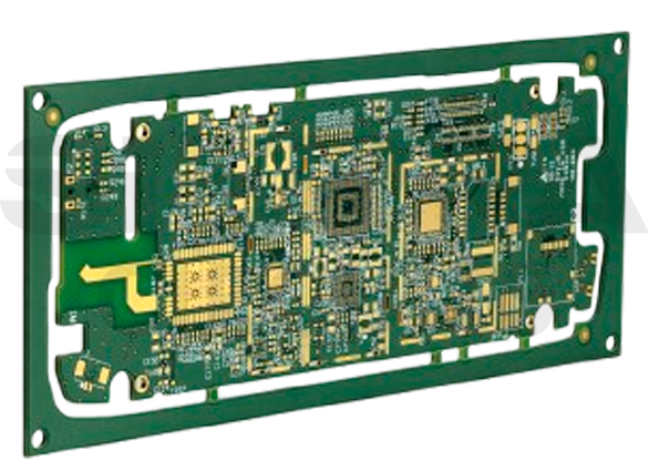
Why and Where Do You Need HDI PCBs?
- Supports finer traces (1.5- 2 mil) and microvias, allowing more components in a smaller
space. - Reduces signal loss, crosstalk, and EMI.
- Shorter signal paths minimize power consumption and enhance efficiency.
- Laser-drilled microvias and buried/blind vias improve board’s structural integrity.
Ideal for:
- Consumer electronics – smartphones, tablets and wearable devices
- Automotive – ADAS, Infotainment and navigation systems
- Aerospace and defense – satellite communication systems, avionics and flight control
systems - Telecommunications – 5G infrastructure, routers, modems and signal boosters

Why Choose Sierra Circuits for your HDI PCB Fabrication?
- We specialize in manufacturing high-density interconnect PCBs, integrating
microvias, fine-pitch components, and high-layer counts with precision. - We provide DFM support and stack-up review to ensure a smooth manufacturing process.
This strategic approach lowers HDI PCB production costs and accelerates
time-to-market. - We have high-precision laser drilling for accurate microvias, blind vias, and buried
vias. Selflearning stack-up scaling and automated imaging system to handle sequential laminations. - Our capabilities extend to 30-layer boards up to 4 lamination cycles. We offer trace
spaces down to 2 mil and holes as small as 2 mil. We also support flex and
rigid-flex HDI technology. - We also specialize in via-in-pad technology, enabling denser routing, reduced
inductance, and improved signal integrity for high-speed and compact designs. - With 30+ years of experience, our team meticulously manages the entire HDI PCB
fabrication and assembly process, ensuring your design meets the highest standards
from prototyping to production
Our expertise:
- Down to 2 mil trace space, 2 mil holes
- Special stack-up help/NPI review
- Blind vias, buried vias, and microvias
- Fine lines and via-in-pad technology
- DFM engineers to validate complex PCB designs
- Dedicated customer portal for real-time project tracking
| Stack-up | Stack-up | |||
|---|---|---|---|---|
| Maximum Layer Count | 30 | 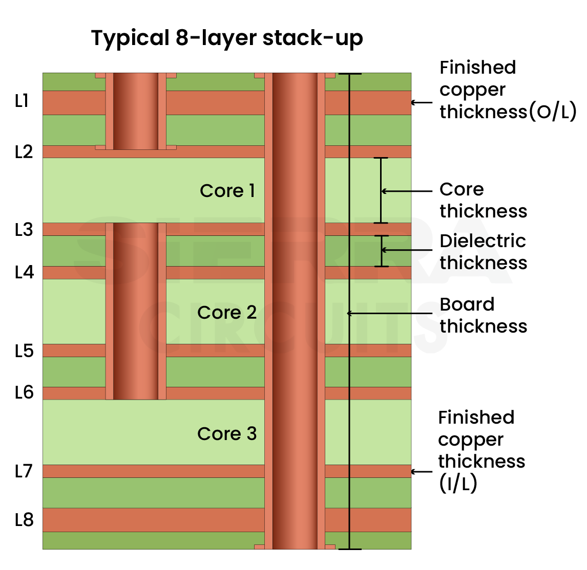 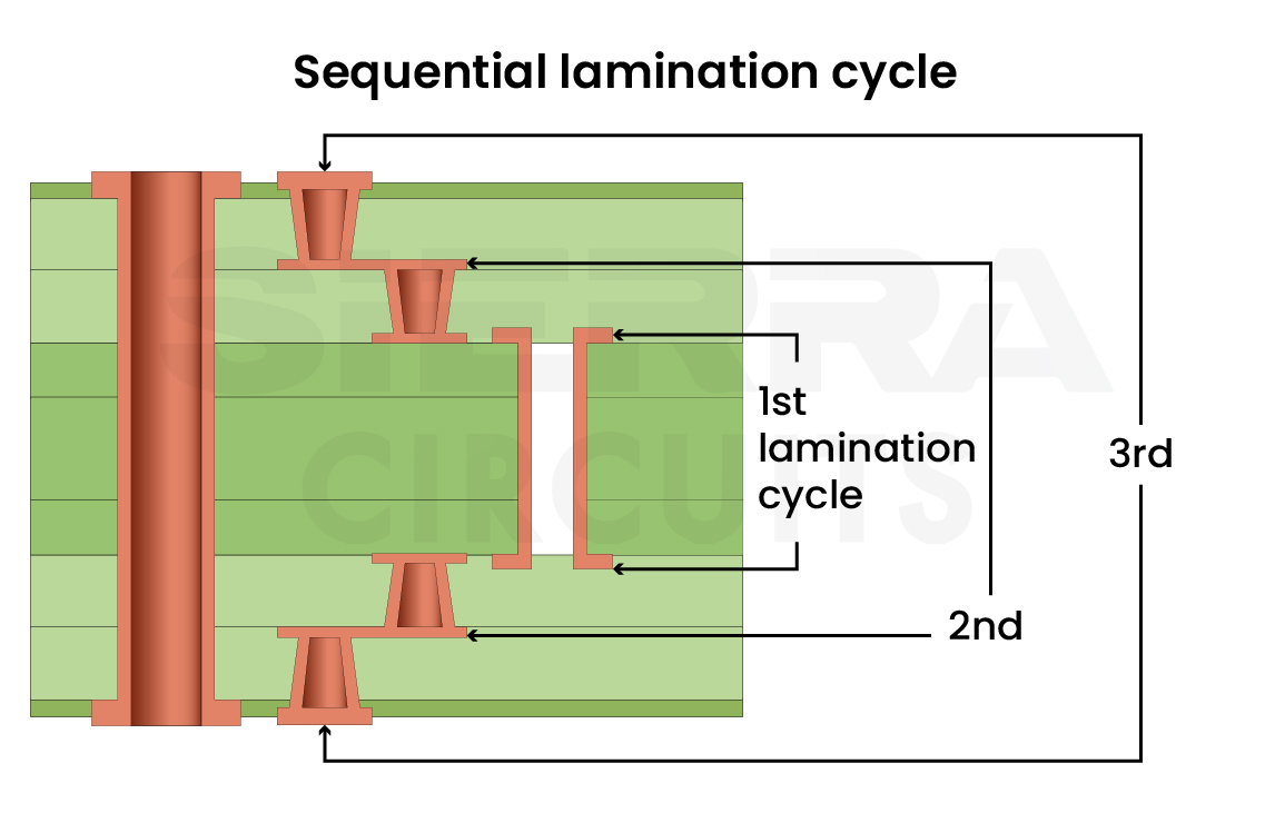 | ||
| Dielectric Material Thickness | 3 mil (0.003 in/0.0762 mm) | |||
| Minimum Board Thickness | 10 mil (0.01 in/0.254 mm) | |||
| Maximum Board Thickness | 250 mil (0.250 in/6.35 mm) | |||
| Maximum Sequential Lamination Cycles | 3 | |||
| Thickness Tolerance (based on board thickness) | ±10% | |||
| Bow and Twist Tolerance | Per IPC spec | |||
| Minimum Core Thickness | 3 mil (0.003 in/0.0762 mm) | |||
| Minimum Starting Copper Foil Weight | 5 micron | |||
| Drill Parameter | Drill Parameter | |||
|---|---|---|---|---|
| Laser Drilled Vias |    | |||
| Minimum Capture Pad Size | 5 mil (0.005 in/0.127 mm) over drill size | |||
| Minimum Laser Drill Size | 5 mil (0.005 in/0.127 mm) | |||
| Laser Aspect Ratio | 0.75:1 | |||
| Largest Laser Drill Diameter | 8 mil (0.008 in/0.2032 mm) | |||
| Blind Vias | Yes | |||
| Buried Vias | Yes | |||
| Stacked Vias | Yes | |||
| Staggered Vias | Yes | |||
| Conductive Filled Vias | Yes | |||
| Non-Conductive Filled Vias | Yes | |||
| Copper-Plate Shut Microvias | Yes | |||
| Mechanically Drilled Vias | ||||
| Minimum Drill Size | 5.9 mil (0.0059 in/0.1499 mm) | |||
| Minimum Pitch | 20 mil (0.02 in/0.508 mm) | |||
| Maximum Mechanical Aspect Ratio | <=10:1 | |||
| Minimum Mechanical Drill to Copper | 7 mil (0.007 in/0.1778 mm) | |||
| Minimum Plated Through Hole Tolerance | ±3 mil (0.003 in/0.0762 mm) | |||
| Minimum Non-Plated Through Hole Tolerance | ±2 mil (0.002 in/0.0508 mm) | |||
| Backdrill to Copper Clearance | 10 mil (0.010 in/0.254 mm) | |||
| Backdrill to Backdrill Clearance | 6 mil (0.0060 in/0.152 mm) | |||
| Minimum Backdrill Oversize Diameter | 8 mil (0.0080 in/0.203 mm) to 10 mil (0.010 in/0.254 mm) | |||
| Minimum Controlled Depth Drilling | More than 1 mil (0.001 in/0.0254 mm) | |||
| Controlled Depth Drilling Tolerance | ±2 mil (0.002 in/0.0508 mm) | |||
| Pad Diameter | Pad Diameter | |||
|---|---|---|---|---|
| Rigid |  | |||
| Inner Layer | Drill+9 mil+class 2 | |||
| Outer Layer | Drill+6 mil+class 2 | |||
| Flex | ||||
| Inner Layer | Drill+10 mil+class 2 | |||
| Outer Layer | Drill+8 mil+class | |||
| Test pad size | ||||
| Minimum Pad Size for Electrical Test | 4 mil (0.004 in/0.1016 mm) | |||
| Minimum Wire Bond Pad Size | 4 mil (0.004 in/0.1016 mm) | |||
| Trace and Space Clearance | Trace and Space Clearance | |||
|---|---|---|---|---|
| Minimum Trace Width (inner layer) | 3.5 mil (0.0035 in/0.0889 mm) |  | ||
| Minimum Trace Width (outer layer) | 3.5 mil (0.0035 in/0.0889 mm) | |||
| Minimum Space Width (inner layer) | 3.5 mil (0.0035 in/0.0889 mm) | |||
| Minimum Space Width (outer layer) | 3.5 mil (0.0035 in/0.0889 mm) | |||
| Controlled Impedance | ±5% | |||
| Minimum Trace Based on Copper Thickness | Minimum Trace Based on Copper Thickness | |||
|---|---|---|---|---|
| 3 microns | 3 mil (0.003 in/0.0762 mm) |  | ||
| 5 microns | 3.25 mil (0.00325 in/0.08255 mm) | |||
| 9 microns | 3.5 mil (0.0035 in/0.0889 mm) | |||
| 1/2 oz | 3.5 mil (0.0035 in/0.0889 mm) | |||
| 1 oz | 4.5 mil (0.0045 in/0.1143 mm) | |||
| 2 oz | 6 mil (0.006 in/0.1524 mm) | |||
| 3 oz | 6.5 mil (0.0065 in/0.1651 mm) | |||
| >3 oz | Contact us | |||
| Solder Mask | Solder Mask | |||
|---|---|---|---|---|
| Colors | Green, Red, and Blue |  | ||
| Minimum Dam/Web Size SMT | 4 mil (0.004 in/0.1016 mm) | |||
| Minimum Dam/Web Size BGA | 3.5 mil (0.0035 in/0.0889 mm) | |||
| Clearance | >0.8 mil (0.0008 in/0.02032 mm) | |||
| Mask-Defined SMT or BGA (Not on the Ground Plane) | Yes | |||
| Mask-Defined Features on the Ground Plane | Yes | |||
| Peelable Solder Mask | Yes | |||
| Silkscreen | Silkscreen | |||
|---|---|---|---|---|
| Inkjet |  | |||
| Color | White | |||
| Minimum Line | 3 mil (0.003 in/0.0762 mm) | |||
| Minimum Height | 25 mil (0.025 in/0.635 mm) | |||
| Screen Printable | ||||
| Colors | White and Black | |||
| Minimum Line | 7 mil (0.007 in/0.1778 mm) | |||
| Minimum Height | 30 mil (0.03 in/0.762 mm) | |||
| Surface Finish | Surface Finish | |||
|---|---|---|---|---|
| Surface Finish Available | HASL, Lead-Free HASL, OSP, ENIG, ENEPIG, Immersion Silver, Electrolytic Soft Gold, and Electrolytic Hard Gold. |  | ||
| Mechanical Parameters | Mechanical Parameters | |||
|---|---|---|---|---|
| Panel Size | 18″×24″ |      | ||
| Minimum Route Cutter Available | 31 mil (0.031 in/0.787 mm) | |||
| Routed Part Size Tolerance | <10 mil (0.010 in/0.254 mm) | |||
| Countersink | Yes | |||
| Counterbore | Yes | |||
| Bevel Angles | 20°, 30°, 45° | |||
| Laser Milling, Depth Tolerance | ± 1 mil (0.001 in/0.0254 mm) | |||
| Laser Routed Thickness | <32 mil (0.032 in/0.813 mm) thick | |||
| Routed Array | Yes | |||
| V Score Angles | 30°, 45°, 60° | |||
| V Score, Edge to Copper | 7 mil (0.007 in/0.178 mm) | |||
| Dicing, Edge to Copper | 5 mil (0.005 in/0.127 mm) | |||
| Edge Castellation, Minimum Drill Via | 10 mil (0.010 in/0.254 mm) | |||
| Edge Plating | Yes | |||
| Recommended Laminate Materials | Recommended Laminate Materials | ||
|---|---|---|---|
| Material Type | Raw Board Manufacturer | ||
| Polyimide | Isola P95 | ||
| Nelco N7000 2 HT | |||
| Arlon 85N | |||
| Ventec VT-901 | |||
| High-Speed FR4 | Isola I-speed | ||
| FR 408HRR | |||
| Nelco N4000-13 | |||
| Nelco N4800-20 | |||
| Tachyon 100g | |||
| Panasonic Meg 6 | |||
| Astra MT77 | |||
| EMC 528 | |||
| EMC 890 | |||
| PTFE | Rogers 5000- Series | ||
| Rogers RT/DUROID Series | |||
| Rogers ULTRALAM 2000 | |||
| Hydrocarbon/Ceramic-Filled | Rogers RO4003 | ||
| Rogers RO4350 | |||
| Rogers 3000,6000 | |||
| Rogers TTM 3, 4, 6, 10, 10i | |||
| Taconics CER-10 | |||
| Taconics RF-35, RF-35A2 | |||
| Taconics RF-60 | |||
| Flex | DuPont Pyralux AP | ||
| DuPont Pyralux LF | |||
| DuPont Pyralux FR | |||
| PCB Testing and Reports | PCB Testing and Reports | |||
|---|---|---|---|---|
| Electrical Testing | Yes |  | ||
| Microsection | Yes | |||
| Solderability | Yes | |||
| Ionic Contamination | Yes | |||
| Time Domain Reflectometry (TDR) Test | Yes | |||
| First Article Inspection (FAI) | Yes | |||
| Hi Pot | Yes | |||
| Test Voltage (Volts) | 40, 250, 500 | |||
| Isolation Resistance (Mohms) | >100 | |||
| Continuity Resistance (Ohms) | <.010 | |||
| Interconnect Stress Testing (IST) | Yes | |||
| D Coupon | Yes | |||
| Quality Reports for HDI PCBs | Quality Reports for HDI PCBs | |||
|---|---|---|---|---|
| IPC 6012, Class 1, 2, 3, and ES | Yes |  | ||
| IPC 6013, Class 1, 2 and 3 | Yes | |||
| 31032 MIL PRF-55110 (on selected materials) | Yes | |||
| UL (94VO) | Yes | |||
| Stack-up | Stack-up | |||
|---|---|---|---|---|
| Maximum Layer Count | 26 | | ||
| MinimumDielectric Material Thickness | 2 mil (0.002 in/0.0508 mm) | |||
| Minimum Board Thickness | 7 mil (0.007 in/0.178 mm) | |||
| Maximum Board Thickness | 200 mil (0.200 in/5.08 mm) | |||
| Maximum Sequential Lamination Cycles | 5 | |||
| Thickness Tolerance (based on board thickness) | ±10% | |||
| Bow and Twist Tolerance | Per IPC spec | |||
| Minimum Core Thickness | 2 mil (0.002 in/0.0508 mm) | |||
| Minimum Starting Copper Foil Weight | 3 micron | |||
| Drill Parameter | Drill Parameter | |||
|---|---|---|---|---|
| Laser Drilled Vias | | |||
| Minimum Capture Pad Size | 4 mil (0.004 in/0.1016 mm) over drill size | |||
| Minimum Laser Drill Size | 4 mil (0.004 in/0.1016 mm) | |||
| Laser Aspect Ratio | 0.75:1 | |||
| Largest Laser Drill Diameter | 6 mil (0.006 in/0.1524 mm) | |||
| Blind Vias | Yes | |||
| Buried Vias | Yes | |||
| Stacked Vias | Yes | |||
| Staggered Vias | Yes | |||
| Conductive Filled Vias | Yes | |||
| Non-Conductive Filled Vias | Yes | |||
| Copper-Plate Shut Microvias | Yes | |||
| Mechanically Drilled Vias | ||||
| Minimum Drill Size | 5.1 mil (0.0051 in/0.1295 mm) | |||
| Minimum Pitch | 15.75 mil (0.01575 in/0.4 mm) | |||
| Maximum Mechanical Aspect Ratio | <=12:1 | |||
| Minimum Mechanical Drill to Copper | 5 mil (0.005 in/0.127 mm) | |||
| Minimum Plated Through Hole Tolerance | ±3 mil (0.003 in/0.0762 mm) | |||
| Minimum Non-Plated Through Hole Tolerance | ±2 mil (0.002 in/0.0508 mm) | |||
| Backdrill to Copper Clearance | 10 mil (0.010 in/0.254 mm) | |||
| Backdrill to Backdrill Clearance | 6 mil (0.0060 in/0.152 mm) | |||
| Minimum Backdrill Oversize Diameter | 8 mil (0.0080 in/0.203 mm) to 10 mil (0.010 in/0.254 mm) | |||
| Minimum Controlled Depth Drilling | More than 1 mil (0.001 in/0.0254 mm) | |||
| Controlled Depth Drilling Tolerance | ±2 mil (0.002 in/0.0508 mm) | |||
| Pad Diameter | Pad Diameter | |||
|---|---|---|---|---|
| Rigid | | |||
| Inner Layer | Drill+8 mil+class 2 | |||
| Outer Layer | Drill+5 mil+class 2 | |||
| Flex | ||||
| Inner Layer | Drill+9 mil+class 2 | |||
| Outer Layer | Drill+7 mil+class 2 | |||
| Test pad size | ||||
| Minimum Pad Size for Electrical Test | 3 mil (0.003 in/0.0762 mm) | |||
| Minimum Wire Bond Pad Size | 3 mil (0.003 in/0.0762 mm) | |||
| Trace and Space Clearance | Trace and Space Clearance | |||
|---|---|---|---|---|
| Minimum Trace Width (inner layer) | 3 mil (0.003 in/0.0762 mm) | | ||
| Minimum Trace Width (outer layer) | 3 mil (0.003 in/0.0762 mm) | |||
| Minimum Space Width (inner layer) | 3 mil (0.003 in/0.0762 mm) | |||
| Minimum Space Width (outer layer) | 3 mil (0.003 in/0.0762 mm) | |||
| Controlled Impedance | ±5% | |||
| Minimum Trace and Spaced Based on Copper Thickness | Minimum Trace and Spaced Based on Copper Thickness | |||
|---|---|---|---|---|
| 3 microns | 2.5 mil (0.0025 in/0.0635 mm) | | ||
| 5 microns | 3 mil (0.003 in/0.0762 mm) | |||
| 9 microns | 3.25 mil (0.00325 in/0.08255 mm) | |||
| 1/2 oz | 3.25 mil (0.00325 in/0.08255 mm) | |||
| 1 oz | 4.5 mil (0.0045 in/0.1143 mm) | |||
| 2 oz | 6 mil (0.006 in/0.1524 mm) | |||
| 3 oz | 6.5 mil (0.0065 in/0.1651 mm) | |||
| > 3 oz | Contact us | |||
| Solder Mask | Solder Mask | |||
|---|---|---|---|---|
| Color | Green | | ||
| Minimum Dam/Web Size SMT | 3 mil (0.003 in/0.0762 mm) | |||
| Minimum Dam/Web Size BGA | 3 mil (0.003 in/0.0762 mm) | |||
| Clearance | >0.5 mil (0.0005 in/0.0127 mm) | |||
| Mask-Defined SMT or BGA (Not on the Ground Plane) | Yes | |||
| Mask-Defined Features on the Ground Plane | Yes | |||
| Peelable Solder Mask | Yes | |||
| Silkscreen | Silkscreen | |||
|---|---|---|---|---|
| Inkjet | | |||
| Color | White | |||
| Minimum Line | 3 mil (0.003 in/0.0762 mm) | |||
| Minimum Height | 25 mil (0.025 in/0.635 mm) | |||
| Screen Printable | ||||
| Colors | White and Black | |||
| Minimum Line | 7 mil (0.007 in/0.1778 mm) | |||
| Minimum Height | 30 mil (0.03 in/0.762 mm) | |||
| Surface Finish | Surface Finish | |||
|---|---|---|---|---|
| Surface Finish Available | HASL, Lead-Free HASL, OSP, ENIG, ENEPIG, Immersion Silver, Electrolytic Soft Gold, and Electrolytic Hard Gold. | | ||
| Mechanical Parameters | Mechanical Parameters | |||
|---|---|---|---|---|
| Panel Size | 12”x18” | | ||
| Minimum Route Cutter Available | 31 mil (0.031 in/0.787 mm) | |||
| Routed Part Size Tolerance | <10 mil (0.010 in/0.254 mm) | |||
| Countersink | Yes | |||
| Counterbore | Yes | |||
| Bevel Angles | 20°, 30°, 45° | |||
| Laser Milling, Depth Tolerance | ± 1 mil (0.001 in/0.0254 mm) | |||
| Laser Routed Thickness | < 32 mil (0.032 in/0.813 mm) thick | |||
| Routed Array | Yes | |||
| V Score Angles | 30°, 45°, 60° | |||
| V Score, Edge to Copper | 7 mil (0.007 in/0.178 mm) | |||
| Dicing, Edge to Copper | 5 mil (0.005 in/0.127 mm) | |||
| Edge Castellation, Minimum Drill Via | 10 mil (0.010 in/0.254 mm) | |||
| Edge Plating | Yes | |||
| Recommended Laminate Materials | Recommended Laminate Materials | ||
|---|---|---|---|
| Material Type | Raw Board Manufacturer | ||
| Polyimide | Isola P95 | ||
| Nelco N7000-2 HT | |||
| Arlon 85N | |||
| Ventec VT-901 | |||
| High-Speed FR4 | Isola I-speed | ||
| FR 408HRR | |||
| Nelco N4000-13 | |||
| Nelco N4800-20 | |||
| Tachyon 100g | |||
| Panasonic Meg 6 | |||
| Astra MT77 | |||
| EMC 528 | |||
| EMC 890 | |||
| PTFE | Rogers 5000- Series | ||
| Rogers RT/DUROID Series | |||
| Rogers ULTRALAM 2000 | |||
| Hydrocarbon/Ceramic-Filled | Rogers RO4003 | ||
| Rogers RO4350 | |||
| Rogers 3000,6000 | |||
| Rogers TTM 3, 4, 6, 10, 10i | |||
| Taconics CER-10 | |||
| Taconics RF-35, RF-35A2 | |||
| Taconics RF-60 | |||
| Flex | DuPont Pyralux AP | ||
| DuPont Pyralux LF | |||
| DuPont Pyralux FR | |||
| PCB Testing and Reports | PCB Testing and Reports | |||
|---|---|---|---|---|
| Electrical Testing | Yes | | ||
| Microsection | Yes | |||
| Solderability | Yes | |||
| Ionic Contamination | Yes | |||
| Time Domain Reflectometry (TDR) Test | Yes | |||
| First Article Inspection (FAI) | Yes | |||
| Hi Pot | Yes | |||
| Test Voltage (Volts) | 40, 250, 500 | |||
| Isolation Resistance (Mohms) | >100 | |||
| Continuity Resistance (Ohms) | <.010 | |||
| Interconnect Stress Testing (IST) | Yes | |||
| D Coupon | Yes | |||
| Quality Reports for HDI PCBs | Quality Reports for HDI PCBs | |||
|---|---|---|---|---|
| IPC 6012, Class 1, 2, 3, and ES | Yes | | ||
| IPC 6013, Class 1, 2 and 3 | Yes | |||
| 31032 MIL PRF-55110 (on selected materials) | Yes | |||
| UL (94VO) | Yes | |||
How to place an order for your HDI PCBs

Trusted by innovators
Engineers at the worlds most innovative companies choose Sierra Circuits for the highest quality HDI PCB manufacturing and assembly, right here in the USA.


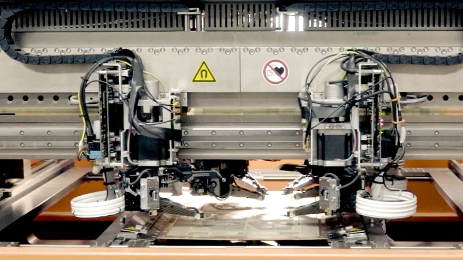
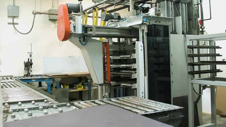

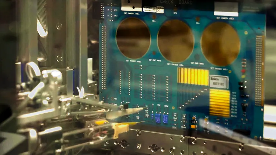
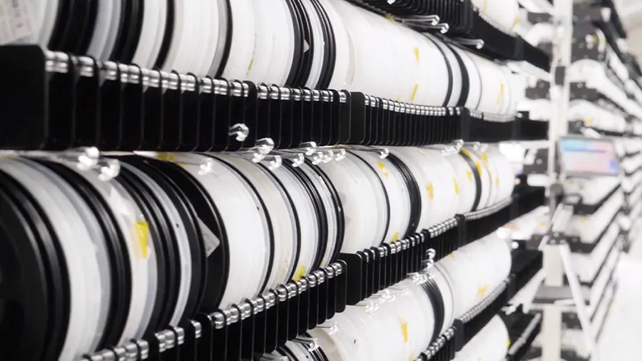


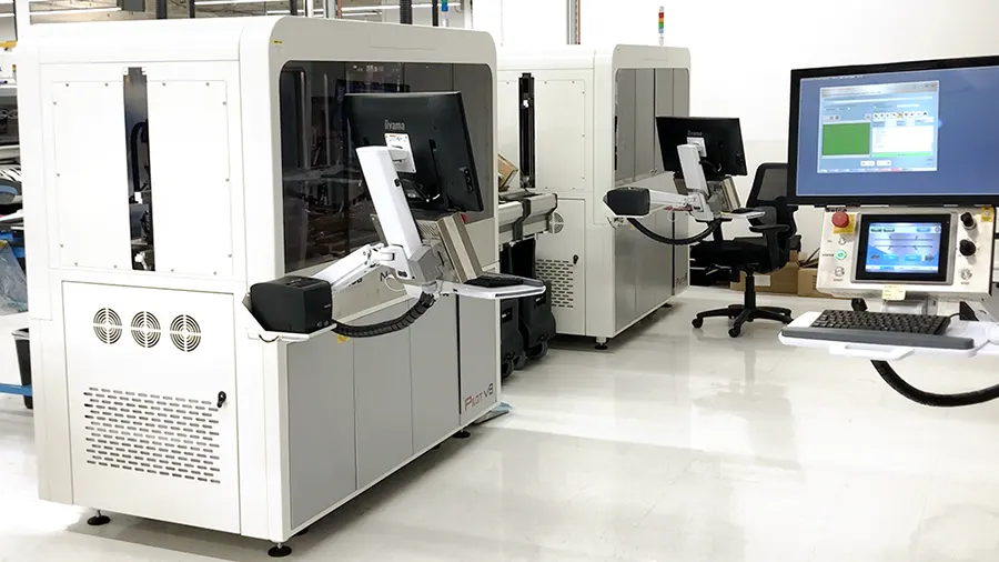
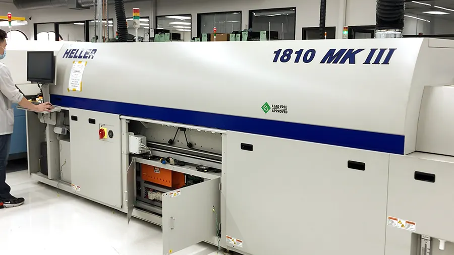
Manufacturing Equipment at Sierra Circuits
Our 70,000 sqft state-of-the-art campus in the heart of Silicon Valley contains the most advanced equipment required for the manufacture and assembly of your PCBs. Whether you’re looking for standard quick turn PCBs or boards with the tightest tolerances, made from exotic metals, there’s a reason Sierra Circuits leads the industry in quality and performance.

Get started with HDI PCBs
We can turn your standard technology PCBs in as fast as in 24 hours.
Start a Custom Quote

Fabrication, Procurement, & Assembly. PCBs fully assembled in as fast as 5 days.
- Bundled together in an entirely-online process
- Reviewed and tested by Engineers
- DFA & DFM Checks on every order
- Shipped from Silicon Valley in as fast as 5 days

Fabrication. Procurement & Assembly optional. Flexible and transparent for advanced creators.
- Rigid PCBs, built to IPC-6012 Class 2 Specs
- 2 mil (0.002″) trace / space
- DFM Checks on every order
- 24-hour turn-times available

Complex technology, with a dedicated CAM Engineer. Stack-up assistance included.
- Complex PCB requirements
- Mil-Spec & Class 3 with HDI Features
- Blind & Buried Vias
- Flex & Rigid-Flex boards