


Contents

On-demand webinar
How Good is My Shield? An Introduction to Transfer Impedance and Shielding Effectiveness
by Karen Burnham
A schematic is a two-dimensional diagram that shows how the components in an electronic circuit are connected. It uses standardized symbols to represent each component, such as resistors, capacitors, and ICs. This allows PCB designers to understand the circuit logic before moving into layout.
Highlights:
- Schematic diagrams use standardized symbols to represent electronic parts like resistors and capacitors.
- Standards such as IEC 60617 and ANSI Y32 define schematic symbols globally.
- Attributes such as resistance, capacitance, and tolerance specify component details.
- Understanding schematics is crucial for creating accurate PCB designs.
What are the standards for schematic symbols?
IEC 60617 and ANSI Y32 are the two major standards that govern schematic symbols. These standards ensure that circuit diagrams use consistent symbols, making them universally readable across industries and design tools.
Let’s look at them in detail:
IEC 60617: The International Electrotechnical Commission (IEC) has issued this standard. It is based on the older standard, British Standard (BS 3939). This database includes over 1750 schematic symbols.
ANSI standard Y32: ANSI stands for the American National Standards Institute. This provides a variety of specialized symbols originally used for aircraft applications. Minor changes were made to the standard to align with IEC.

Design for Manufacturing Handbook
11 Chapters - 96 Pages - 90 Minute ReadWhat's Inside:
- Annular rings: avoid drill breakouts
- Vias: optimize your design
- Trace width and space: follow the best practices
- Solder mask and silkscreen: get the must-knows
Download Now
What are the different schematic symbols in circuit design?
Resistors, capacitors, diodes, ICs, power supply, and ground reference are a few of the commonly used schematic symbols in circuit design. In the example below, a basic circuit is built using a battery, a resistor, and an LED.

These electronic components are connected through nets/traces. Each component has a symbol with different attributes.
The attributes of a resistor will be its reference designator, value, size, symbol, voltage rating, wattage, and footprint. Similarly, the battery and the LED will have their attributes.
The table below shows the names, symbols, and their corresponding reference designators used in the circuit. The designators, BT, R, and LED represent battery, resistor, and light-emitting diode, respectively. These reference designators help us to identify the components.

By knowing the symbols and their reference designators, you can interpret any circuit and build it accordingly.
These are the most common schematic symbols:

Schematic symbols indicate the type of component, but they don’t explain how it behaves. That information comes from the component’s values and attributes.
What are values and attributes in schematics?
Consider the basic schematic diagram shown in the previous section. The circuit shows that the positive terminal of the battery is connected to the light-emitting diode through a resistor, R. But there is no other information about the attributes of these components (the resistance value of the resistor and the voltage capacity of the battery).
The schematic diagram should provide this additional information to ensure that appropriate components are selected. The resistor should have its resistance value expressed in ohms(Ω). The battery should state its potential difference (voltage) expressed in volts.
Other components are described in different terms. For example, capacitors are differentiated by their capacitance value expressed in farads (F), and inductors are differentiated by their inductance value expressed in henrys (H).
Sometimes additional attributes can be given to the symbols (power ratings and tolerances, etc). This helps us identify the appropriate components for the circuit. Some of the common attributes of a component are:
- The symbol with the shape and pins
- Values such as ohms, capacitance, and inductance of the components
- Reference designator, for example, U1, R1, C1, etc.
- Maximum operating conditions example: maximum voltage for capacitors, maximum wattage for resistors
- Tolerances example: For resistance: ±1%, ±5%
- Manufacturer part number (MPN)
- Component footprints (for resistors: 0402, 0805; for 8-pin IC: SOIC8)

Fill out the form:
The international system of units
Attribute values can vary from very small to extremely large units. To avoid filling circuit diagrams with long, repeating strings of zeros for values like 1,000,000,000 or .0000000001, we use the international system of units (SI) for values.
| Prefix | Symbol | Value | Powers of 10 |
|---|---|---|---|
| tera | T | 1,000,000,000,000 | 1012 |
| giga | G | 1,000,000,000 | 109 |
| mega | M | 1,000,000 | 106 |
| kilo | k | 1,000 | 103 |
| milli | m | 0.001 | 10-3 |
| micro | µ | 0.000001 | 10-6 |
| nano | n | 0.000000001 | 10-9 |
| pico | p | 0.000000000001 | 10-12 |
What are the differences between schematic and wiring diagrams?
| Feature | Schematic diagram | Wiring diagram |
|---|---|---|
| Purpose | Shows how the circuit functions logically using wires and symbols | Shows pictorial representation of an electrical circuit; gives details on the relative location and arrangement of devices |
| Focus | Electrical relationships and signal flow | Real-world routing and placement of wires |
| Representation of components | Uses standardized electronic symbols (resistors, capacitors, ICs) | Shows actual representations or simplified shapes of components |
| Detail level | Less detailed. Provides logical connections only | More detailed. Includes wire lengths, colors, and physical locations |
| Use case | Circuit design, simulation, and PCB layout creation | Installation, troubleshooting, and field wiring |
Need help creating clear and accurate schematic diagrams? Explore our PCB design support.

How to read a PCB schematic?
Reading a schematic involves identifying components, their interconnections, and understanding the circuit’s functional intent. The schematic diagram gives the following information:
- Components used
- Electrical connections between component pins
- Operating conditions such as voltage, current, and tolerances
- Special instructions for single-ended traces, differential pairs, and positions of the components, such as placement of decoupling capacitors, crystals, and so on.
- Block diagram
- Revision history (if any)
Here are the common elements of a schematic diagram:
1. Schematic nets: These define how components are interconnected in a circuit. The line between the two interconnected components is called a net.

Read our post on schematic and netlist checks to ensure error-free designs, to understand schematic netlist and its generation using Altium Designer.
2. Junctions and nodes: A junction is formed when two or more wires intersect at a point. This junction is represented by placing a little dot (node) on the point of intersection, as shown in the image below.
To learn more, read Network Theory for Better PCB Design and Development.
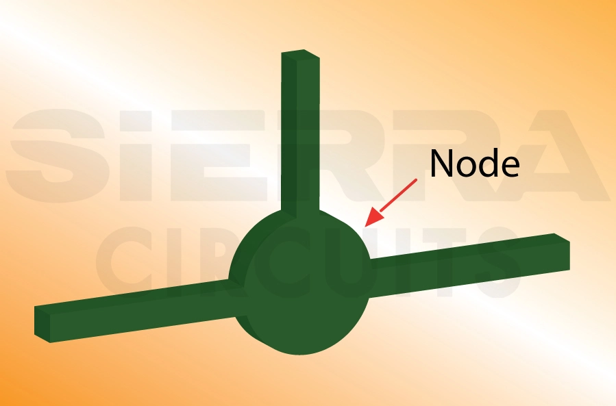
Nodes help us to identify the connection among the wires intersecting a point. The absence of a node at a junction means two separate wires are just passing by without any electrical connection.
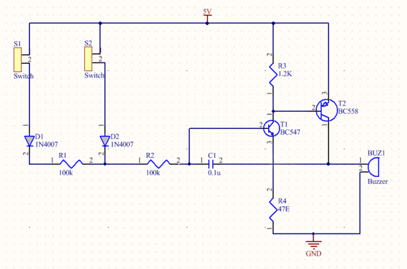
3. Net names: In order to make the schematic diagram more legible, the nets are labeled with their names rather than drawing lines to show the connectivity. It is assumed that the nets with the same name are connected even though there isn’t any visible connection made.
The image below shows an example of a schematic diagram in which nets are labeled with their names.

What is the difference between a schematic diagram and a layout?
| Feature | Schematic Diagram | PCB Layout |
|---|---|---|
| Purpose | Defines the logical connections between components on a circuit board (rigid or flex). Shows how components are electrically connected. | Shows the exact physical placement of components on the PCB and the physical wires (traces) connecting them. |
| Representation of components | Uses standardized component symbols (resistors, capacitors, ICs). | Shows actual component footprints (pads, holes, copper areas). |
| Detail level | Less detailed. Focuses on electrical logic, not physical constraints. | More detailed. Considers spacing, trace width, clearances, and manufacturability. |
| Use cases | Circuit design, documentation, and troubleshooting. | PCB fabrication, assembly preparation, and final manufacturing. |

How do you create a schematic diagram?
Schematic creation involves generating component symbols, placing them correctly, defining attributes, and ensuring logical connectivity.
If a design uses a hierarchical schematic, where numerous functional diagrams are interrelated with each other, then it defines the relationship between groups of components in different schematic diagrams.
Below are the 4 steps involved in schematic diagram creation using a PCB CAD tool:
1. Symbol generation: This process involves drawing the body of the component, adding pins and pin numbers, defining the symbol attributes, and assigning a footprint.
The symbols are sometimes readily available in the PCB CAD software. To learn more, check out How to Create a Schematic and Symbol Library in KiCad.
2. Component symbol placement: The body of the component symbol is created by placing closed symbol shapes in the schematic library editor.
3. Pin numbering: Pins define the connection points on the component for the incoming and outgoing signals. Pin numbering is made to ensure the connections shown in the schematic end up connected properly by copper on the PCB.
4. Symbol attributes: It mainly consists of category, value, manufacturer, manufacturer part number, and supplier. It is recommended that every symbol on your circuit have its own unique designator so that every part is easily identifiable.
What are the rules for drawing schematic diagrams?
Stick to these guidelines when designing a schematic diagram:
- Represent electrical connections with lines, and connect intersecting lines only when a node is present.
- Limit node connections to a maximum of three lines.
- Assign names to nets; nets with the same name are assumed to be connected.
- Write pin numbers, polarity, values, and net names horizontally.
- Place inputs on the left side and outputs on the right side.
- Organize the schematic into functional blocks.
- Position pin numbers on the outside of the symbol graphic.
- Place sheet-connection symbols at the extreme left or right edges of the page.
- Locate the title block in the lower-right corner of the first sheet, including:
- Title
- Part number
- Revision (if any)
Schematic diagrams primarily consist of component symbols and the lines that represent the connection between the components. Understanding the schematic diagram is very important for designers in order to design a successful PCB.
We have now covered the basic concepts related to schematic symbols and schematic diagrams. Comment below if you have any queries on schematics.
Have questions about schematic diagrams? Post your queries on SierraConnect. Our PCB experts will answer them.
About Milan Yogendrappa : Milan Y is an electronics and communication engineer with over 6 years of experience in developing and editing technical articles related to PCB design, manufacturing, and assembly. He is currently the editor-in-chief at Sierra Circuits.


Start the discussion at sierraconnect.protoexpress.com