


Contents

On-demand webinar
How Good is My Shield? An Introduction to Transfer Impedance and Shielding Effectiveness
by Karen Burnham
Propagation delay (tpd) in PCBs is the time taken by a signal to travel through a unit length of a transmission line. The propagation of electrical signals through PCB traces is not instantaneous; it is subject to a delay. This delay results in timing errors, data skew, clock, and data mismatches, and causes reliability issues.
Highlights:
- Factors affecting propagation delay include dielectric constant, stray capacitance, and impedance mismatch.
- Material selection, critical length, and signal speeds are critical for reducing propagation delay.
- Techniques like meandering, trace length tuning, and controlled impedance routing can be used to reduce tpd in your designs.
- Propagation delay is typically less on PCB outer layers than inner layers, and matching characteristic impedance between traces and components reduces unwanted delay and reflections.
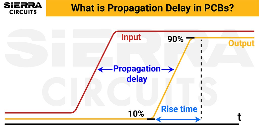
What is propagation delay in a PCB?
Propagation delay is the time delay experienced by a signal to reach its destination (source to load). It is the function of the dielectric constant (Er) and the trace geometry.
Total signal propagation time = tpd × transmission line length (𝐋trace)
It is expressed in time per unit length (ns/ps per inch or cm)
tpd is directly proportional to trace length and inversely proportional to the signal speed. It is prevalent in high-speed designs and hampers signal integrity.
What causes propagation delay?
Propagation delay occurs due to inconsistent dielectric constant, parasitic capacitance, impedance mismatch, and signal reflections.
Let’s see their impact in detail:
1. Inconsistent dielectric constant

Materials with inconsistent dielectric constants tend to exhibit more signal dispersion and impedance discontinuities. Practically, materials with higher Dk (>4) exhibit greater signal losses and propagation delay compared to substrates with lower dielectric constants. Signal dispersion is a phenomenon in which high-speed signals experience distortion. It occurs when different signal components travel at different speeds through a medium.
| Material | Er | Ereff | Vmicrostrip (in/ns) |
Vstripline (in/ns) |
tpd microstrip (ps/in) |
tpd stripline (ps/in) |
|---|---|---|---|---|---|---|
| Vacuum or air | 1 | 1 | 11.8 | 11.8 | 85 | – |
| Isola 370HR | 4.0 | 2.92 | 6.90 | 5.9 | 145 | 170 |
| Isola I-SPEED | 3.64 | 2.69 | 7.20 | 6.18 | 139 | 162 |
| Isola I-META | 3.45 | 2.57 | 7.36 | 6.35 | 136 | 158 |
| Isola Astra MT77 or Tachyon 100G or Rogers 3003 | 3.0 | 2.28 | 7.8 | 6.8 | 128 | 147 |
| Rogers 4000 series | 3.55–3.66 | 2.63–2.7 | ~7.20 | ~6.20 | ~139 | ~161 |
To learn how to select the right laminates, download the High-Speed Material Design Guide.

High-Speed Material Design Guide
6 Chapters - 19 Pages - 30 Minute ReadWhat's Inside:
- Importance of choosing the right material for your high-speed design
- Parameters that affect material selection
- Effect of dielectric constituents on your circuit board
- Characteristics of high-speed materials
- Effect of resin content and glass weave structure on your PCB
Download Now
2. Stray/parasitic capacitance
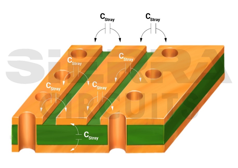
Parasitic capacitance increases the capacitive load of the signal, resulting in tpd and signal integrity issues. Stray capacitance can occur due to capacitance between traces, adjacent ground plane, and free space.
3. Impedance mismatch
Controlled impedance traces can minimize signal reflections and thereby reduce propagation delay. The physical parameters of the trace, i.e., trace width and thickness, distance from other copper features, dielectric constant, and dielectric thickness or distance to the reference plane of the board material, all contribute to the impedance of a trace.
The non-uniform impedance between the driver and the transmission line leads to signal reflections and prolonged propagation delay.
4. Signal reflections
Signal reflections due to the abrupt change in impedance at signal transitions, such as interfaces or connectors, can cause some signals to reflect back toward the source. These reflections can lead to overlapping signal transitions and result in timing uncertainties and skews.

Fill out the form:
What is the difference between transmission delay and propagation delay?
| Parameter | Transmission delay | Propagation delay |
|---|---|---|
| Definition | Time required to push all bits of a packet onto the medium | Time required for a signal to travel from the sender to the receiver |
| Depends On | Packet size and data rate | Physical distance and signal propagation speed |
| Formula | Packet size ÷ Bandwidth | Distance ÷ Propagation speed |
| Influenced By | Network bandwidth, serialization rate | Medium type (copper, fiber, air) and dielectric properties |
| Typical Impact | Affects how quickly data begins transmission | Affects the end-to-end latency of the signal |
| Layer Association | Data link and network transmission behavior | Physical layer signal behavior |
| Example | Sending a 1,500-byte Ethernet frame over a 100 Mbps link | Signal traveling 10 km through fiber at ~2×10⁸ m/s |

Transmission delay and propagation delay can be used interchangeably, but they need to be handled differently when the system is required to be analyzed in analog/digital aspects.
Watch our webinar on strategies to optimize propagation delay in your PCB design.
How propagation delay affects the signal speed in a PCB trace
Propagation delay slows down the signal traveling on a trace, resulting in timing errors.
When a PCB operates at a high frequency, the traces behave like a transmission line. Controlled impedance calculations are very important for these traces so that signal reflections, crosstalk, noise, and ground bounce can be mitigated.
These issues require special attention since they may impose a threat to signal quality, causing the entire system to fail.
How is signal speed calculated?
The signal speed for the microstrip and stripline is calculated as:

Where,
Vc is the velocity of light in vacuum/air.
Vc = 3 x 10⁸ m/s = 186,000 mil/s = 11.8in/ns
For a microstrip configuration, you have one reference plane below and air on the top, and therefore, Ereff is the effective dielectric constant between air and the dielectric material.
Ereff is an effective dielectric constant for microstrips, and its value lies between 1 and Er.
Ereff = (0.64 Er + 0.36)
It signifies that the signal speed on a circuit board is less than that in the air. If the Er of the PCB material is 4, then the signal speed on a stripline design is half of that in air, about 6in/ns.
How to calculate propagation delay?
On PCB transmission lines, tpd is given by:

Mathematically, the time delay is equal to 1/v, where v is the speed of the signal in a PCB transmission line.
In vacuum/air, it’s equal to 85 ps/in.
Propagation delay in striplines is given by:

Propagation delay for microstrips is given by:

Propagation delay of a circuit with multiple interconnects

Total propagation delay of a system with multiple interconnects is given by:
∑(Delays through each section of the circuit) = tpd = (tpd_𝟏+tpd_𝐯𝟏+tpd_𝟐+tpd_𝐯𝟐+tpd_𝟑)
Circuits have many interconnects that include signal, ground, and power traces, vias, connectors, and differential pairs.
What’s the impact of characteristic impedance (Z0) on tpd?
Higher characteristic impedance results in faster propagation velocity, which minimizes propagation delay by allowing signals to propagate quickly. Maintaining uniform characteristic impedance between transmission lines and components/connectors on your board is of utmost importance to minimize signal reflections.
Every transmission line in your PCB has a particular characteristic impedance, and it is the ratio of the transmission signal’s voltage amplitude to its current amplitude as it travels over a conductor.
For a lossless transmission line, characteristic impedance, Z0 =√(𝑳/𝑪)
tpd = trace length (L) / velocity of propagation (v)
Signal propagation speed: v=𝟏/√ LC
Propagation delay per unit length can be given by: tpd = 1/v =√ LC
The characteristic impedance calculated using this method is an approximate value. This is because we have considered the lossless transmission and neglected losses due to the skin effect and copper roughness.
For better results, use Sierra Circuits’ Impedance Calculator. This tool uses a 2D numerical solution of Maxwell’s equations for PCB transmission lines to calculate the characteristic impedance.

Relation between critical length and tpd
For analog signals, the critical length (lc) is defined as one-fourth of the wavelength of the highest signal frequency contained in the signal.
Let the maximum frequency in an analog signal be 𝐟𝐦 Hz and 𝐯 be the signal speed, then,
Wavelength of the highest frequency signal, 𝛌𝐦= 𝐯/𝐟𝐦
tpd=𝟏/𝐯
Therefore, 𝛌𝐦=𝟏/(tpd 𝐟𝐦)
For analog signals, the critical length lc is defined as one-fourth of the highest signal frequency content in the signal
Critical length = 𝛌𝐦/𝟒=𝟏/(𝟒 tpd 𝐟𝐦)
Ideally, the trace length should always be less than the critical length to avoid signal distortion.
For digital signals, the maximum value of lc is the line length over which signal propagation time is half of its fastest rise/fall time, tr
lc= (tr/2)×(1/tpd)
tpd= tr/(2lc)
Hence, from the above equations,
lc=(tr/2)×(1/tpd)
tr= 2lctpd
For a signal with rise time tr, the 3 dB bandwidth is given by the following rule:
3dB bandwidth, BW3dB=(0.35)/tr = (0.35)/(2lc ×tpd )

What’s the effect of propagation delay on a shortline?
On a short line, the propagation delay is so small that the entire line responds almost instantaneously. As a result, the line behaves like a lumped element rather than a transmission line, with minimal waveform distortion or phase shift.
A shortline is when the trace length l< lc/(1.5) = 𝛌𝐦/6. Signal delay and impedance mismatching rarely matter if you have shorter traces and they don’t undergo propagation delay.
To expedite the process of computing the critical length, Sierra Circuits has developed a tool called Bandwidth, Rise Time, and Critical Length Calculator.
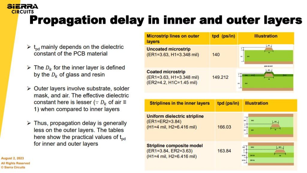
Propagation delay in inner and outer layers
Propagation delay mainly depends on the dielectric constant of a PCB material.
The Dk for the inner layer is defined by the Dk of glass and resin, whereas the Dk of the outer layers involves substrate, solder mask, and air. The effective dielectric constant here is less (∵ Dk of air ≡ 1) when compared to the inner layers.
Thus, propagation delay is generally less in the outer layers. The tables here show the practical values of tpd for the inner and outer layers.

7 ways to reduce propagation delay in your PCB designs
1. Choose a suitable dielectric material
FR4 can be used for high-speed PCB design when the layers are laminated with high-speed laminates such as Rogers. At high frequencies, FR4 experiences dispersion, which increases the speed and decreases the propagation delay.
Electromagnetic absorption in Fr4 generates more signal attenuation for the traces associated with it. Thus, high-speed laminates are used below high-speed traces along with FR4 laminates, especially at frequencies above 5GHz.
Stick to these guidelines while selecting the materials:
- Low 𝐷𝑘 ≤ 4
- Low 𝐷𝑓 (∼0.001)
- Uniform 𝐷𝑘
- Always compare the dispersion characteristics of your material with a well-known low-dispersion material. A few of the low-dispersion materials include Rogers, Panasonic Megtron 6 (M6), and Elite EM-355D with FR4 laminates
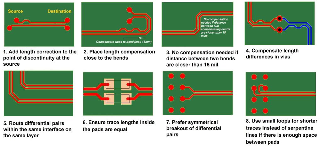
2. Meander the traces for length matching
Meandering is done to match the length of the traces in a net. It is always good to meander differential traces together.
So, how do you decide which traces have to be meandered?
- Identify the longest signal trace and meander the remaining traces in a net to sync the signal across all the traces.
- Adjust the clock trace length that connects the components in the given net to reach the output state before the next clock pulse.
- Delay the clock pulse by the time until the ICs can rise to the full voltage applied.
- Implement the same number of vias for each trace.
- Set traces with uniform lengths/geometry on each layer
In a signal net, traces with mismatched lengths are always matched to the trace having a maximum length. Meanders are added to the shorter traces so that their length can be increased.

8 length matching tips for differential pairs
3. Optimize the signal delay in vias
Always consider delays caused by vias. This adds to the total signal tpd. Use via physical dimensions to calculate inductance (𝐋𝐯), capacitance (C𝐯), and impedance (Z𝐯)
The propagation delay of a via, tpd_𝐯𝐢𝐚= √(𝐋𝐯 C𝐯 )
For a differential pair, you need to calculate the effective dielectric constant, inductance, and capacitance of the via geometry and tpd for both lines

4. Implement a solid return path
Return paths provide a low-impedance line to the high-speed signals. It is very crucial for a signal to complete the loop to maintain signal integrity. Splits, voids, and gaps in the return path can cause impedance mismatches and increase signal delay. A larger return loop can introduce parasitic inductance, which can delay the return current flow and cause propagation delay.
- Always implement a solid plane underneath the trace through the entire length with no splits or cuts.
- If you don’t want to have a solid plane, use a thick return trace, where the trace thickness is 3 times the dielectric height.

5. Focus on pin-package delays
When a signal arrives on a pin/pad of a particular component, it still needs to traverse the exposed conductor path along with the interior of the component package. While traversing the signal trace and the bond wire associated with the internal circuitry, the signal experiences parasitic inductance and capacitance, which affect its travel speed in the bond wire compared to the trace.
The bond wires also have different geometries that add to the signal delay on different pins/pads. Ask your manufacturer for the pin-package delay associated with a particular component. It is mentioned in picoseconds (ps) or as a length in mm/microns. This length should be considered while performing any delay/length tuning with signals in differential pairs or single-ended signals.
6. Watch your clock skew
When clock and signal traces have different lengths, it results in a timing mismatch called clock skew. Ignoring this problem may lead to wrong data being latched. The clock delay should be greater than the greatest delay in the data signals.
7. Follow the standard high-speed design rules
- Route high-speed traces on outer layers for lower propagation delay
- Incorporate 3W to 5W separation between controlled impedance traces
- Consider placing critical components in close proximity to each other in order to minimize trace length and delay.
- Implement proper termination techniques, such as using series or parallel termination, to match impedance and minimize reflections.
- Along controlled impedance traces, avoid abrupt bends, tees, and changes in trace width to reduce impedance variations and signal reflections.

High-Speed PCB Design Guide
8 Chapters - 115 Pages - 150 Minute ReadWhat's Inside:
- Explanations of signal integrity issues
- Understanding transmission lines and controlled impedance
- Selection process of high-speed PCB materials
- High-speed layout guidelines
Download Now
Managing propagation delay with controlled impedance traces
Different trace geometries/structures can be used for controlled impedance traces. The trace configurations we are discussing here are based on IPC standard 2141A.
- Wire microstrip: It is made up of a discrete insulated wire separated by a fixed distance over a ground plane. The dielectric can be either the insulation wall of the wire or a combination of this insulation and air.
- Surface microstrip: In a two-sided PCB design with a ground plane on one side, a signal trace on the other side can be designed for controlled impedance. This trace structure is known as surface microstrip or simply microstrip.

- Embedded/symmetric stripline: In a multi-layer PCB, this arrangement implements the signal trace between a power and a ground plane. The return current path for a high-frequency signal trace is located above and below the signal trace on the planes. So, the high-frequency signal remains inside the PCB, resulting in fewer emissions and shielding from other spurious signals.

Note: The ground plane is at zero potential with a low-impedance reference plane having a larger area.
- Coplanar structure: A coplanar waveguide structure has the signal trace and the return path conductor on the same layer of the PCB. The signal trace is at the center and is surrounded by the two adjacent outer ground planes; it is called ‘coplanar’ because these three flat structures are on the same plane. The PCB dielectric is located underneath. Both microstrips and striplines may have a coplanar structure.

To learn how to design transmission lines without propagation delay, see designing transmission lines with controlled impedance in high PCB layouts.
Parameters to consider before choosing a high-speed PCB design software
If you are using a software tool that considers only the length mismatch, then you can easily calculate the correct length mismatch value for a given substrate. This length mismatch is equal to the timing mismatch multiplied by signal velocity (in/ns) in the given substrate. A good PCB design software should offer the following things to target propagation delay:
- Interactive routing capabilities
- Smart length tuning
- IPP enhancements (instant access to new and existing functions)
- Dynamic data model (to speed up netlist creation)
- User-friendly
Key takeaways:
- Propagation delay is critical for accurate and timely signal transfer on a PCB. Delay can lead to timing errors, data skews, and clock and data mismatches, affecting performance and reliability.
- The dielectric constant, stray capacitance, impedance mismatch, and signal reflections affect the propagation delay.
- Signal speed for both strip lines and microstrips is influenced by the effective dielectric constant and electromagnetic signal speed in vacuum/air
- Managing propagation delay in PCBs that have multiple interconnects requires summing delays through various sections.
- Proper matching of characteristic impedance between transmission lines and components/connectors on the PCB helps minimize signal reflections and ensure efficient signal propagation.
- Critical length is crucial for preventing signal distortion and maintaining signal quality.
- Propagation delay varies between the inner and outer layers of the PCB and is generally less on the outer layers.
- Choose materials with low-dispersion properties to effectively reduce propagation delay.
- Employ techniques such as adjusting trace length, incorporating meandering, considering via delay, and ensuring a consistent return path to control propagation delay.
- Implementing controlled impedance traces and proper design practices is highly recommended for minimizing signal reflections and propagation delay.
Let us know in the comments if you need any high-speed PCB design assistance. Our experts will be happy to help you.

About Mohamed Faheemuddin : Mohamed Faheemuddin is a mechanical engineer. His passion for electronics drew him to the PCB industry. With an experience of over 3 years in the PCB industry, he specializes in developing articles for engineers and hardware designers.


Start the discussion at sierraconnect.protoexpress.com