Contents

On-demand webinar
How Good is My Shield? An Introduction to Transfer Impedance and Shielding Effectiveness
by Karen Burnham
During DesignCon 2022, we interviewed Matthew Harms of EMA Design Automation to understand more about model extractions and simulations. Watch the video to find out his insights.
Matthew Harms is an electrical engineer from Canada and has been with EMA as an application engineer since 2003 and as the application engineer team leader since 2018. At EMA, he specializes in design side issues pertaining to part management, circuit simulation, signal integrity, and power integrity but is conversant in all facets of ECAD design.
What are the challenges in today’s PCB design in terms of speed and power?
Matthew: There are lots of challenges. Everyone wants two things: faster speed and less power. With the speed increasing, you have to be concerned about neighbors, the materials, proximity and closures, delivery, and all kinds of problems with speed and power. Make sure you have adequate power, and your margins are good as well as your decoupling strategy. So there are lots of things to worry about with higher speed and lower power all the time.
What are the characteristics of high-speed, low-loss board materials and does it influence material selection?
Matthew: We would select and gather the material properties from our vendors like Sierra Circuits who manufacture the board. We would get those numbers and then put them into our software and run a simulation based on that and make sure they work. For the selection of materials, we talk to the board manufacturer about what we are doing and they recommend board materials based on cost. It is always a balance of cost and functionality. Make sure that you get what you need for what you are paying.
Can you share a few guidelines on effective component placement in the PCB layout?
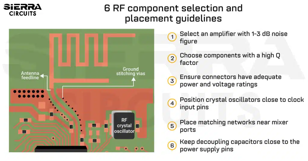
Matthew: Component placement is related to power and speed. It would be best to place things as close as you can to each other. So the closer the things are together, the less chance they have of problems happening to them, either from neighbor nets or from themselves just getting reflection. Therefore, close placement is kind of a general rule. It does not always work. You need to do a simulation to figure out the suitable placement with functionality. So for decoupling capacitors, it would be near your power supply. Closeness is the usual key and then routing those out directly with low inductance to your power points is pretty important.
What are the issues and critical elements involved in PCB data management?
Matthew: PCB data management is a little bit complex but we try to make it as simple as possible. There is a lot to be concerned about when it comes to your parametric data like the value, the tolerance, the manufacturer part number, the internal part number for your part data, and where do they sit. It is critical to manage well and locate centrally. Managing task distribution among engineers and handling not only your part data but also design files is important as well. Your libraries, your footprints, and your design files are all that need to be managed. In the larger groups, permission to access is critical and for smaller groups, this is not as important, but design management is a big part of what everybody needs to be concerned with.
What are the key differences between model extractions and simulations?
Matthew: Model extraction is trying to turn something physical into something that could be simulated. That would be a trace on your board or a plane on the board, something that exists on the board which you want to simulate. You can not just give your board file to a simulator, and say, go simulate. It needs to be extracted before. What extraction means is that you are turning that physical part in your design into something mathematical. So you want to turn that copper line into a model, something that could be put into a simulator and the simulator understands mathematical things. Normally those are S parameter files, which is an industry standard for just communicating, how signals move basically, and how that compares to simulation. The simulation would then be compiling those models, taking them altogether and throwing some sort of signal stimulus at it, and seeing what it does. So you have to actually activate those extracted models and see what comes out the other end.
What are the latest tools and simulations you would recommend for power integrity analysis?
Matthew: There are certainly many in the industry but we will talk about ours here. The power integrity solutions that we have will help you figure out whether the decoupling capacitors are useful or not, that is a big one. Engineers often overdesign. They put so many capacitors on because they can afford them and they don’t know what will go wrong. The consequences can be big. They usually put too many and that causes a waste of components, a waste of space. We have software that can help the engineer figure out how many is good enough when the problem will be solved. The other one that we would have is your DC power, which allows you to look at your resistive losses on the board and see how much current and power is lost just on the fact that it has to travel from one place to another and experiences those resistive losses. So being able to quantify that, measure it, look at it, and determine it is something that we offer and is called power DC.

Signal Integrity eBook
6 Chapters - 53 Pages - 60 Minute ReadWhat's Inside:
- Impedance discontinuities
- Crosstalk
- Reflections, ringing, overshoot and undershoot
- Via stubs
Download Now
How do you design a functional power delivery network and overcome challenges such as multiple voltage requirements, rising power consumption, etc.?
Matthew: You can certainly see that power delivery networks are getting larger and more complex all the time. Engineers have more voltage levels to worry about and where they come from and how they travel around your board. It can just be very confusing because your nets and signal names are going to change all the time too, and it is tough to keep track of. So we have a tool called Allegro PowerTree. That would help you track what that signal is. Basically, it is coming in the connector from the wall to the board and it comes at 24 volts. It spreads like a tree and goes everywhere and figures out where this all goes. It touches other components and is a DC to DC converter. You can say that takes your 24V and turns it into 5 and 3V. Thus, it becomes a little tree, branches off for you automatically. Just keeping track of that whole tree can become challenging and is something that engineers often do just in spreadsheets with pen and paper. But we have a tool that tells you where the root is and we go and get the rest of that tree for you and give you a nice diagram for it.
What are some key features of 3D FEM and what are the challenges associated with it?
Matthew: 3D FEM is finite element modeling. This is a technique for extracting your physical design into mathematical form. It uses a mathematical set of modeling and is extremely accurate. It focuses on accuracy. To model extremely high frequencies, it is very good. The downside or the trade-off you are going to get with that is it is computationally intensive to get that model. It takes a lot of computational power, you might need a special machine to even run that has a lot of horsepower. The second trade-off is that it takes a lot of real-world time to achieve that result.
It takes perhaps hours, days, or weeks to get you a model out of that. We again have a solution again for this. Our solution in that space is called clarity and clarity works very hard at parallelizing, that is making parallel paths, making good use of all your cores that you have in your CPU, and having them each work and then bring that work together so that you can maximize the capabilities of your computer. You will hopefully get fast and accurate results.
What is the significance of field solvers and can you explain the next generation 3D field solver?
Matthew: Field solvers are used for extraction. When you have traces on your board, you need to solve them with field solvers. There are so many different field solvers. It is an incredibly detailed field that you can get into just studying to analyze a lot of things. It is a mathematical representation of physical form. At Cadence, there are probably at least five or six different kinds of field solvers you could use. They each have their benefits and the benefits could be cheaper to purchase from us, it could be faster simulation, greater accuracy, and those are all trade-offs that you want to make with your field.
There is not much more to gain in terms of accuracy in next generation 3D field solvers. It can take a long time to run, like days for simulation. If you can cut that in half, it allows the engineer to get the results twice as fast and get moving on to other things more quickly. So the battlefront in 3d field solving specifically is speed, how fast you can get that out. The model accuracy is the same.
High-Speed PCB Design Guide
8 Chapters - 115 Pages - 150 Minute ReadWhat's Inside:
- Explanations of signal integrity issues
- Understanding transmission lines and controlled impedance
- Selection process of high-speed PCB materials
- High-speed layout guidelines
Download Now
About Poulomi Ghosh : Poulomi is a microwave engineer specializing in EMI, EMC, RF, and high-speed electronics. As a senior technical writer at Sierra Circuits, she creates advanced engineering articles and webinars for hardware engineers and PCB designers.


