


Contents

On-demand webinar
How Good is My Shield? An Introduction to Transfer Impedance and Shielding Effectiveness
by Karen Burnham
A composite or nested-feedback amplifier is typically used when a single op-amp can’t meet all performance requirements. It ensures high gain, wide bandwidth, and low noise. A poorly implemented composite op-amp can oscillate or lose precision due to layout parasitics or incorrect feedback values.
As a PCB designer, you should consider adding one when the design demands:
- High DC accuracy and high slew rate or bandwidth
- Low noise and offset at the input, but high output current or voltage swing
- Wide bandwidth at high closed-loop gain
- Heavy, capacitive, or fast-edge loads without sacrificing stability
In this article, you’ll learn what composite amplifiers are, how they differ from cascaded amplifiers, and practical design and layout guidelines you should follow to ensure stable, high-performance operation.
Highlights
- A composite architecture pairs a low-offset, low-noise voltage-feedback op amp front end with a high-speed or high-current output stage.
- The global feedback network sets the overall gain; local gain around the output stage mainly tunes bandwidth and stability.
- Overall stability is highly sensitive to feedback resistor values, capacitive loading, and PCB layout, especially around the inverting node and feedback loop.
- PCB layout should prioritize short feedback paths, tight coupling between stages, effective decoupling, and careful handling of high-impedance nodes to preserve bandwidth.
What is a composite amplifier in PCBs?
A composite amplifier is a two-stage amplifier block that behaves like a single op amp. It is built by nesting a high-power or high-speed amplifier inside the feedback loop of a precision amplifier.

In the above schematic,
- AMP1 is the precision front end (usually a voltage feedback amplifier). It has the following features:
- Low input offset and bias current
- Low noise and distortion
- Sets the overall closed-loop gain
- AMP2 is in the output stage (typically a current feedback amplifier or high-current op amp/driver). Its features include:
- High slew rate and wide bandwidth
- High output voltage and/or current capability
- May have its own local feedback loop, but sits inside the global loop
From a system perspective, the composite block behaves like a single non-inverting op amp. The overall gain is determined entirely by the global feedback network, independent of the internal stage partitioning.
Since the output of AMP2 is fed back to AMP1 through the global feedback network, the precision front end actively corrects the DC and low-frequency errors of the output stage. On the other hand, the output stage supplies the power, speed, and load-driving capability that the precision device alone cannot deliver.
Single op amp vs. composite architecture
| Characteristic | Single precision op amp | Single high-speed/ high-current op amp | Composite amplifier (precision + driver) |
|---|---|---|---|
| DC precision | Excellent | Low | Excellent (set by front end) |
| Bandwidth at high gain | Limited | Better, but may still trade off with gain | Extended by splitting the gain across two stages |
| Output current/voltage drive | Limited | High | High (provided by driver stage) |
| Noise | Low | High | Low at low and mid frequencies (set by the precision front end) |
| Distortion | Higher at large signal amplitudes | Low at high speed, but limited by poor DC linearity | Low (driver distortion corrected by feedback) |
| Design and layout complexity | Lowest | Moderate | Highest (needs careful stability/layout handling) |
Use a composite amplifier when you require:
- High gain and MHz-level bandwidth.
- High output current or large peak-to-peak voltage, and precision.
- Integration of a precision voltage-feedback amplifier (VFA) with a current-feedback amplifier (CFA) or power driver without sacrificing accuracy.
Composite amplifier vs. cascaded amplifier
Both amplifiers use multiple stages, composite amplifier’s gain is set by a single global feedback loop, whereas the cascaded amplifier’s gain is the product of the individual stage gains.

These amplifier architectures are often confused, but their gain behavior and feedback structure differ in important ways. The table below summarizes the differences:
| Amplifier type | How gain is determined | Feedback structure | System-level behavior |
|---|---|---|---|
| Composite | Set by a single global feedback loop (R₁/R₂) | Multiple amplifiers inside one shared loop | High precision with DC-error correction; bandwidth extension via gain splitting; distortion of the output stage corrected by the front end. |
| Cascaded | Approximately the product of individual stage gains | Each stage typically has its own independent feedback (or no feedback) | Errors and noise accumulate stage-to-stage; limited system-level error correction; bandwidth is often reduced at high overall gains. |
To learn how to avoid assembly delays and extra costs, download the Design for Assembly Handbook.

Design for Assembly Handbook
6 Chapters - 50 Pages - 70 Minute ReadWhat's Inside:
- Recommended layout for components
- Common PCB assembly defects
- Factors that impact the cost of the PCB assembly, including:
- Component packages
- Board assembly volumes
Download Now
How does gain work in a nested-feedback amplifier?
The overall composite gain is defined entirely by the global feedback network, R1 and R2.

The circuit behaves like a single non-inverting operational amplifier with a closed-loop gain:
ATotal=1+R1/R2
The local feedback around AMP2 (set by R3 and R4) does not directly change the overall gain. Instead, it primarily affects:
- The effective gain that AMP1 is forced to provide
- Bandwidth distribution
- Loop stability and phase margin
- Noise and distortion allocation between stages
If AMP2’s gain is increased via R3 and R4:
- AMP2’s output initially increases
- The global feedback loop (R1/R2) senses the increased composite output
- The loop corrects by reducing AMP1’s effective gain
- The final composite output remains unchanged
When designing a composite amplifier for your layout:
- Keep R1 and R2 unchanged, as they set the composite amplifier’s closed-loop gain and directly define system-level behavior.
- Use R3 and R4 (around AMP2) as internal tuning components to control loop stability, bandwidth allocation, and noise and distortion characteristics.
- Avoid modifying R3 and R4 without performing a stability analysis. Any adjustment to these components shifts internal pole-zero locations and alters the gain distribution between stages.
How does a composite amplifier extend bandwidth?
The composite architecture splits the required system gain across multiple stages instead of forcing a single amplifier to provide the entire gain. This allows each amplifier to operate at a higher bandwidth.

For any op amp, closed-loop bandwidth (BW) is limited by its gain-bandwidth product (GBWP):
BW≈ GBWP/Gain
As gain increases, available bandwidth decreases. A composite architecture distributes the total gain between two amplifiers, allowing each stage to operate at a lower closed-loop gain and therefore higher bandwidth.
At unity gain, the bandwidth improvement is small. However, at higher gains, performance improves significantly. For example, instead of using a single amplifier with a gain of 10, splitting it evenly (about 3.16 × 3.16) can deliver 2× to 4× more bandwidth.
How to use VFAs and CFAs in a composite architecture?
One of the most effective design patterns for high-performance PCB analog systems is combining a voltage-feedback amplifier at the input with a current-feedback amplifier at the output, both operating within a single composite feedback loop.

The VFA (AMP1) serves as the precision front end, where accuracy matters most. It offers:
- Low input offset voltage and bias currents
- Low noise performance
- High loop gain for excellent DC and low-frequency accuracy
This ensures the signal is conditioned with maximum precision before being passed to the output stage.
The CFA (AMP2) acts as the high-speed output driver providing:
- Extremely high slew rate
- Wide bandwidth with the correct feedback resistor (RF)
- Strong output current for driving cables, ADC inputs, probes, and low-impedance loads
This allows the system to maintain fast edges and large signal swings without sacrificing stability.
The VFA and CFA form a composite amplifier that:
- Looks like a low-noise, precision amplifier at the input
- Behaves like a fast, high-current driver at the output
- Prevents thermal and dynamic stress in the CFA output stage from corrupting the sensitive VFA input stage
The CFA feedback loop is not optional. The feedback resistor (RF) directly controls stability. Removing it or shorting it will lead to oscillations.
8 common challenges when designing a composite amplifier
Working closely with PCB designers, we have learned that the following challenges are commonly experienced when designing nested-feedback amplifiers.
1. Noise and distortion
At low frequencies, noise and distortion are dominated by the precision front end, but as frequency increases, the output stage becomes the primary contributor. Any gain peaking in the frequency response typically shows up as overshoot, elevated wideband noise, or EMI problems.
Solution:
Minimize parasitic inductance and capacitance in the global feedback path and maintain tight physical coupling between stages to reduce parasitics.
2. Stability and phase margin
Multiple feedback loops (global + AMP2 local) mean extra poles and zeros in the loop gain. Capacitive loads (cables, long traces, DAC outputs, scope probes) can easily erode phase margin.
Typical symptoms:
- Peaking in the frequency response
- Ringing or overshoot in the step response
- Full-blown oscillation at high frequency
Solution:
Control phase margin through proper loop compensation by including feedback capacitors and series output resistors for capacitive loads.

3. Capacitive sources and loads (especially with CFAs)
Current-output DACs, long traces, and probe capacitances add parasitics at the inverting input and capacitive load at the output.
For CFAs in particular, either of these can push the crossover frequency into regions where the amplifier already has a large phase shift.
Generally, a low-range feedback capacitor is added across the RF to introduce phase lead and stabilize the loop. Unfortunately, looping feedback paths that add inductance and parasitics can negate the intended stabilization and reintroduce peaking or oscillation.
Solution:
Place CFA feedback components directly at the amplifier pins and isolate capacitive sources and loads with series resistors.
4. Incorrect feedback resistor values on CFAs
CFA datasheets specify an optimal RF value for each closed-loop gain.
If RF is too low, loop gain may be too high at frequencies where the CFA already has a large phase shift. This leads to overshoot or oscillation.
If RF is too high, bandwidth collapses unnecessarily.
Solution:
Use datasheet-recommended CFA feedback resistor values and avoid value edits that alter feedback impedance.
5. Unequal or poorly chosen gain splitting
Composite amplifiers often rely on splitting the gain between AMP1 and AMP2 to maximize bandwidth while keeping the system stable. This only works well if the output stage has equal or higher GBWP than the front end.
If the front end is much faster or much slower than the output stage, mismatched gain distribution can create peaking, oscillations, or a need for additional compensation. Under those conditions, PCB parasitics become even more influential.
Solution:
Distribute gain so each stage operates at a moderate closed-loop gain. Assign more gain to the slower stage to preserve phase margin.
6. Offset and noise dominated by the wrong stage
Ideally, the front-end amplifier (AMP1) is the dominant contributor to the system’s overall noise and DC offset, because the errors from AMP2 are largely attenuated by the global feedback loop.
But when the global loop has limited bandwidth or poor phase margin, AMP2’s noise, distortion, and thermal drift start to leak into the output. Insufficient supply decoupling or strong thermal variation at AMP2 can easily translate into spurious noise or slow output drift.
Solution:
Provide low-impedance decoupling directly at each amplifier’s supply pins and ensure adequate low-frequency loop gain so the precision amplifier remains in control of DC accuracy and low-frequency noise.
7. Thermal coupling between precision and power stages
The output stage (AMP2) often dissipates far more power than the precision front end. If the two devices are placed too close together without thermal isolation, changes in AMP2 temperature can modulate AMP1’s offset and drift, degrading precision performance.
Good thermal spacing and heat spreading are essential to avoid these effects on real boards.
Solution:
Use copper pours and thermal vias to spread and steer heat away from the precision front end while avoiding direct thermal paths between stages.
For more heat dissipation tips, see 12 PCB thermal management techniques to reduce PCB heating.
8. Difficult probing and debugging
Key nodes (especially the inverting input and inner feedback paths) are high impedance and sensitive to probe capacitance and lead inductance.
An oscilloscope probe in the wrong place can make a stable loop ring or oscillate and mislead the debug process.
Solution:
Provide dedicated test points and use low-capacitance probing techniques to avoid measurement-induced loop instability.
Maintaining uniform impedance is critical for a stable composite amplifier performance. Any variations can disrupt feedback behavior and reduce phase margin.
Sierra Circuits fabricates and assembles PCBs with consistent impedance and a tolerance of ±5%. Visit our controlled impedance capabilities to learn more.
What are the consequences of a poorly implemented nested-feedback amplifier?
A composite amplifier that is not carefully tuned can introduce serious performance problems that are often difficult to diagnose and correct. Common consequences include:
- Unexpected oscillations or ringing, especially at high frequencies or when driving capacitive loads, cables, or connectors.
- Gain peaking and overshoot, which reduce phase margin and can lead to measurement errors or false signal content.
- Degraded DC accuracy, with offset and drift higher than predicted from the selected precision front-end amplifier.
- Increased noise and distortion, particularly when the global loop cannot fully correct the output stage’s errors due to limited bandwidth or improper compensation.
- Thermal drift and long-term instability, as power dissipation in the output stage alters operating points and consumes the available error budget.
- High sensitivity to component tolerances and parasitics, where small changes in feedback resistors, compensation capacitors, layout, and component parasitics, or load conditions can push the system into instability.
- Difficult bring-up and validation, with circuits that appear stable in simulation but require multiple board spins and empirical tuning to behave correctly in hardware.
Common PCB layout mistakes that lead to composite op-amp oscillation
Composite amplifiers most often oscillate due to PCB layout errors that add parasitic capacitance or inductance, disrupt feedback paths, or couple noise and heat between precision and power stages.
Watch out for these layout mistakes:
- Long or indirect feedback routing.
- Shared ground paths between AMP1 and AMP2.
- Missing output isolation resistor.
- Decoupling capacitors are placed far from power pins.
- Feedback traces routed near high-dv/dt power nodes.
- Poor thermal isolation between power and precision amplifier stages.
Even one of these mistakes can turn a stable schematic into an oscillating PCB.
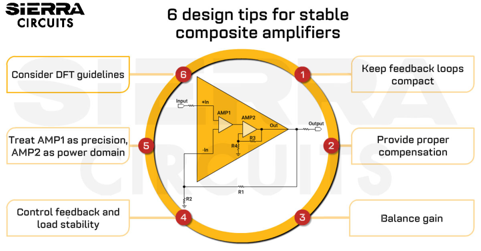
6 PCB design recommendations for a stable composite amplifier
Composite amplifiers’ efficiency is achieved through careful gain distribution and compensation, proper handling of high-speed drivers, capacitive loads, and clear separation of precision and power domains.
Follow these guidelines when you’re implementing a composite amplifier in your design:
1. Keep feedback loops compact and clean
- Place AMP1 and AMP2 close together.

Feedback loop of an amplifier. - Route the global feedback from the AMP2 output back to AMP1, inverting the input of AMP1:
- Keep the trace as short and direct as possible.
- Avoid stubs or unnecessary vias.
- Route away from noisy digital or switching nets.
- Never route feedback over split planes.
- Consider this feedback path like a critical RF net, not a generic analog trace.
2. Provide proper compensation for amplifier stability
- Use low-value capacitors (calculated from loop-gain requirements) across feedback resistors to control high-frequency gain.
- Add a series output resistor (5–50 Ω) to isolate capacitive loads.
- Place local compensation caps around the output stage.
- Include optional snubber networks when additional damping is needed.
3. Balance gain across amplifier stages
- Begin with roughly equal gain per stage.
- Shift the gain toward the slower stage if the phase margin becomes tight.
4. Control feedback and load stability in high-speed driver stages
- If AMP2 is a CFA or fast driver:
- Use the recommended RF values from the datasheet for the intended gain.
- Place RF and a feedback capacitor directly at the amplifier pins with minimal loop area.
- For capacitive loads (DAC outputs, cables, filters):
- Use series output resistors, snubbers, or small compensation caps to keep phase margin healthy.
- Avoid hanging long, wide copper areas directly on sensitive inverting nodes.
- Avoid wide pours directly attached to high-speed outputs.
- Do not route outputs parallel to sensitive inputs.
5. Treat AMP1 as the precision and AMP2 as the power domain
For AMP1 (precision front end):
- Keep input traces short, symmetric, and well isolated.
- Guard high-impedance nodes to prevent leakage.
- Avoid routing near switching regulators or high-current paths.
- Provide a dedicated low-noise ground reference.
- Keep it physically separated from hot or noisy components (FETs, inductors, drivers).
- Use precision VFAs for sensors, DAC buffers, and instrumentation signals.
- Avoid thermal gradients across sensitive input resistors.
For AMP2 (driver):
- Use wider traces or pours for load currents.
- Keep output routing short and tightly controlled.
- Implement dedicated, low-impedance power and ground planes.
- Ensure high-current returns do not share ground with AMP1.
- Provide solid decoupling on each supply pin (local 0.1 µF + nearby bulk cap).
- Add copper area or thermal vias if it dissipates significant power, and avoid heat flowing straight into AMP1.
- Use wideband/high-current drivers for cables, ADC inputs, and actuators.
- Prioritize stability first, bandwidth second, when selecting and configuring AMP2.
- Use a continuous analog ground plane.
- Provide separate return paths for AMP1 and AMP2.
- Place bulk and ceramic decoupling caps within 2-3 mm of each supply pin.
- Do not place the output stage adjacent to the precision input stage.
6. Consider DFT guidelines
- Add accessible probe/test points on the input and output of the composite block.
- Avoid routing high-speed outputs under shielding cans unless isolation and accessible test points are provided.
For more DFT tips, download the Design for Testing Handbook.

Design for Testing Handbook
7 Chapters - 28 Pages - 45 Minute ReadWhat's Inside:
- PCB testing strategies
- Guidelines to design and place a test point for FPT
- Directives to make your board ICT compatible
- Benefits and drawbacks of various testing methods
- Defects that you can identify through board testing
Download Now
How should PCB designers validate a nested-feedback amplifier?
Composite amplifier behavior is validated by combining simulation with prototype PCB testing, time- and frequency-domain measurements, and thermal stress evaluation under worst-case conditions.
To ensure a composite amplifier behaves as intended on a PCB, designers typically:
- Simulate with real models
- Use SPICE models of both amplifiers and real feedback networks.
- Run AC (Bode), transient, and noise analysis to check gain, phase margin, overshoot, and noise.
- Validate the design
- Pay attention to how actual parasitics introduced by vias, connectors, and cables affect amplifier stability.
- Measure step response and frequency response
- Look for overshoot, ringing, or unexpected resonances.
- Sweep load capacitance if the output will drive cables, ADC inputs, or configurable loads.
- Implement thermal and long-term testing
- Run the composite amplifier at worst-case load and ambient conditions.
- Monitor drift, noise, and offset changes as temperature and time vary.
Careful validation is key to avoiding stability and performance issues in composite amplifier designs.
Talk to a PCB expert: Book a meeting or call us at +1 (800) 763-7503.
Pros and cons of a composite amplifier
Pros:
- Precision and speed: Composite amplifiers provide excellent DC accuracy with wide bandwidth, fast slew rates, and strong load-drive capability that are difficult to achieve with a single op amp.
- Superior DC performance: The precision amplifier sits at the front of the global feedback loop. Hence, the composite retains low offset, low drift, low noise, and clean DC linearity, even when the output stage is a high-power or high-speed device.
- Improved load-driving capability: Placing the driver amplifier inside the feedback loop greatly boosts output current and voltage swing while keeping accuracy defined by the precision stage. The result is a strong load drive for heavy or low-impedance loads without losing precision.
- Stable output offset and reduced trim effort: The global feedback loop corrects the output stage’s offset through negative feedback:
- Self-heating and load-dependent offset errors in the power stage are largely suppressed.
- DC output offset is more stable across load changes.
- In many cases, you can reduce or eliminate the need for manual offset trimming, cutting circuit board BOM cost, and simplifying calibration.
- Higher slew rate and better dynamic response: Composite configurations can effectively multiply the slew rate of the front-end amplifier. The driver stage handles large voltage swings and fast edges, while the precision stage linearizes the overall response so the system behaves like a faster, more linear op amp.
- Flexible architecture using standard components: Composite designs let engineers build a custom high-performance amplifier from readily available op amps, selecting one device optimized for precision and another optimized for current or bandwidth, then combining them inside a single feedback loop without needing a specialized or proprietary IC.
This is especially valuable in power amplifiers, DAC buffers, and wideband signal paths where both accuracy and fast transitions are required.

Cons:
- Reduced effective gain: Nested negative feedback improves stability and accuracy, but reduces the raw gain available from each stage. If the gain is not properly planned between AMP1 and AMP2, the output can appear weaker than expected.
- Potential increase in output resistance: Depending on the feedback topology, the composite loop can raise the output resistance compared to a dedicated power driver. This can slightly reduce output voltage stability when driving heavy or low-impedance loads.
- Greater design and layout complexity: Multiple nested feedback loops make composite amplifiers far more sensitive to parasitics, component tolerances, and routing. Stability issues are harder to diagnose, and debugging misbehavior can require more iteration.
- Stricter PCB layout requirements: Achieving stability demands careful attention to feedback routing, decoupling, grounding, and thermal planning. Small layout mistakes, especially around the inverting node or CFA feedback path, can introduce ringing, oscillation, or loss of precision.
Even with these drawbacks, the benefits generally outweigh the disadvantages in demanding analog and power applications. This is why they continue to see growing use in power amplifiers, RF/microwave signal chains, precision DAC buffers, and other high-performance analog sections where a single op amp can’t meet all the requirements on its own.
Composite amplifiers deliver precision and power in a single stage, as long as the PCB layout preserves feedback integrity and stability. By considering the composite amplifier as a single high-performance block with careful loop routing and proper CFA feedback handling, you can achieve wide bandwidth, high gain, and excellent accuracy with standard op amps.
About the technical reviewer:
Abhishek Chari is the Team Lead for PCB Design at Sierra Circuits, with 6 years of experience specializing in high-speed PCB layouts and advanced HDI technologies. He possesses deep expertise in leading EDA tools, including Altium Designer, Cadence Allegro, Eagle PCB, and KiCAD.
Have questions about printed circuit boards? Post your queries on SierraConnect. Our PCB experts will answer them.

About Pooja Mitra : Pooja Mitra is an electronics and communication engineer. With an experience of over three years in the PCB industry, she creates industry-focused articles that help electrical and PCB layout engineers.


Start the discussion at sierraconnect.protoexpress.com