Speak to an Account Manager
![]() +1 (800) 763-7503
+1 (800) 763-7503
Related Categories — IPC » PCB Manufacturing
Annular Ring Explained by a PCB Manufacturer
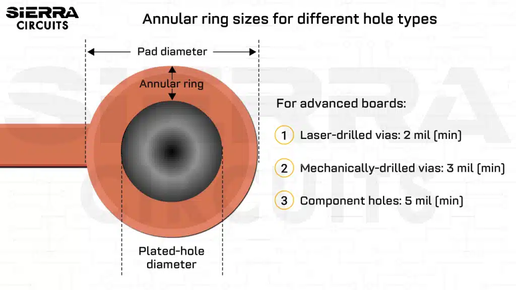
Annular rings are one of the biggest concerns of PCB designers. You know that you may place your via right in the middle of the pad in the design files, but it just does not mean that you will 100 percent avoid tangencies, or even worse, breakouts. Let’s talk about annular rings, shall we?
PCB Design
Microwave PCB Material Selection and CPW for Signal Integrity
Designing microwave boards involves meticulous selection of PCB materials, precise etching, and careful management of electromagnetic effects. These ... more »
PCB Design
Try the KiCad Plugin for an Instant PCB Quote
Get instant PCB fab and assembly cost estimation for your designs through Sierra Circuits’ KiCad quote plugin. You ... more »
KiCad Tutorials
Annular Ring Explained by a PCB Manufacturer
Annular rings are one of the biggest concerns of PCB designers. You know that you may place your ... more »
PCB Design
Microwave PCB Material Selection and CPW for Signal Integrity
Designing microwave boards involves meticulous selection of PCB materials, precise etching, and careful management of electromagnetic effects. These ... more »
PCB Design
Try the KiCad Plugin for an Instant PCB Quote
Get instant PCB fab and assembly cost estimation for your designs through Sierra Circuits’ KiCad quote plugin. You ... more »
KiCad Tutorials
How to Pick RF PCB Materials: 7 Important Factors to Consider
When designing RF PCBs, selecting the right material is pivotal for achieving optimal board performance. The properties of ... more »
High Speed
How to Choose the Right HDI PCB Materials
Choosing the right dielectric material for a PCB is important no matter what application you’re working. However, the ... more »
HDI / Blind & Buried Vias
Via Filling Techniques Designers Need to Know for PCB Fabrication
PCB via filling is a technique in which the plated hole is filled with a conductive or non-conductive ... more »
PCB Manufacturing
Solder Mask Layer in PCBs: Top 4 DFM Guidelines
After PCB fabrication, the copper traces on the board typically face the risk of oxidation and corrosion due ... more »
PCB Manufacturing
How to Optimize Your PCB Designs for Testing by Harry Kennedy
Harry Kennedy, an electrical engineer and technical specialist at Altair, has shared his expertise in optimizing PCB designs ... more »
PCB Design
The Future of PCB Etching by Laurent Nicolet
Laurent Nicolet, the Vice President of Business Units Electronics at the Schmid Group, talks about the future of ... more »
PCB Experts


Fabrication, Procurement, & Assembly. PCBs fully assembled in as fast as 5 days.
- Bundled together in an entirely-online process
- Reviewed and tested by Engineers
- DFA & DFM Checks on every order
- Shipped from Silicon Valley in as fast as 5 days

Fabrication. Procurement & Assembly optional. Flexible and transparent for advanced creators.
- Rigid PCBs, built to IPC-6012 Class 2 Specs
- 2 mil (0.002″) trace / space
- DFM Checks on every order
- 24-hour turn-times available

Complex technology, with a dedicated CAM Engineer. Stack-up assistance included.
- Complex PCB requirements
- Mil-Spec & Class 3 with HDI Features
- Blind & Buried Vias
- Flex & Rigid-Flex boards