Speak to an Account Manager
![]() +1 (800) 763-7503
+1 (800) 763-7503
Related Categories — IPC » PCB Manufacturing
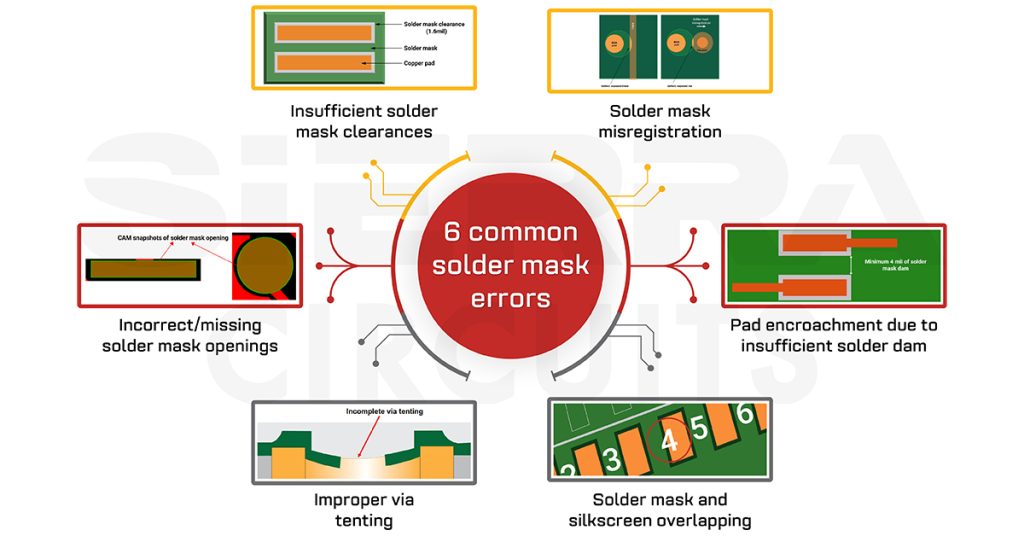
6 Common Solder Mask Errors Every PCB Designer Should Know
A solder mask is an insulation layer that covers conductive areas such as traces and pads. Inappropriate solder layer application […]
PCB Design
Advantages of Ordering PCB Prototype and Bulk Production from a Single Fab House
Choosing the same fab house for PCB prototypes and bulk production has many advantages, such as better DFM ... more »
PCB Manufacturing
How to Design and Build a Hybrid PCB Stack-Up
A hybrid stack-up construction enhances your PCB’s performance and cost-effectiveness by combining different materials or technologies. It helps ... more »
PCB Manufacturing
6 Common Solder Mask Errors Every PCB Designer Should Know
A solder mask is an insulation layer that covers conductive areas such as traces and pads. Inappropriate solder ... more »
PCB Design
Advantages of Ordering PCB Prototype and Bulk Production from a Single Fab House
Choosing the same fab house for PCB prototypes and bulk production has many advantages, such as better DFM ... more »
PCB Manufacturing
How to Design and Build a Hybrid PCB Stack-Up
A hybrid stack-up construction enhances your PCB’s performance and cost-effectiveness by combining different materials or technologies. It helps ... more »
PCB Manufacturing
How Sequential Lamination is Performed to Manufacture HDI PCBs
Sequential lamination is a process of fabricating a circuit board using subsets composed of copper and dielectric layers. ... more »
HDI / Blind & Buried Vias
Benefits of Choosing Turnkey PCB Manufacturing and Assembly from a Single Facility
Turnkey PCB manufacturing services include design review, fabricating bare boards, procuring components, assembly, and testing of your prototype. ... more »
PCB Assembly
How to Get a Quickturn PCB Prototype in USA
With standard technology—single lamination, through-hole, two, four, six, and eight-layer boards... a one to three-day turn is fairly ... more »
PCB Manufacturing
Wet PCB Etching Using Acidic and Alkaline Methods
Copper etching is one of the important processes in PCB manufacturing. We can simply say that wet PCB ... more »
PCB Manufacturing
High Speed PCB Materials: Rogers 4350B and Panasonic Megtron 6
There has been extensive research on the development of low loss materials in the past few decades with ... more »
High Speed
How to Troubleshoot and Repair Your PCBs
By troubleshooting and repairing a PCB, you will extend the lifespan of the circuit, which is both cost-efficient ... more »
PCB Assembly


Fabrication, Procurement, & Assembly. PCBs fully assembled in as fast as 5 days.
- Bundled together in an entirely-online process
- Reviewed and tested by Engineers
- DFA & DFM Checks on every order
- Shipped from Silicon Valley in as fast as 5 days

Fabrication. Procurement & Assembly optional. Flexible and transparent for advanced creators.
- Rigid PCBs, built to IPC-6012 Class 2 Specs
- 2 mil (0.002″) trace / space
- DFM Checks on every order
- 24-hour turn-times available

Complex technology, with a dedicated CAM Engineer. Stack-up assistance included.
- Complex PCB requirements
- Mil-Spec & Class 3 with HDI Features
- Blind & Buried Vias
- Flex & Rigid-Flex boards