Speak to an Account Manager
![]() +1 (800) 763-7503
+1 (800) 763-7503
Related Categories — HDI / Blind & Buried Vias » PCB Design » PCB Manufacturing
How Sequential Lamination is Performed to Manufacture HDI PCBs
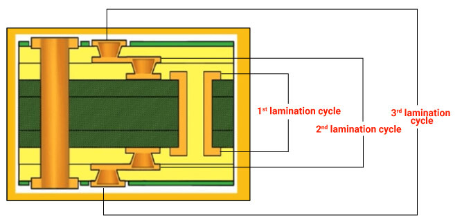
Sequential lamination is a process of fabricating a circuit board using subsets composed of copper and dielectric layers. This process […]
HDI / Blind & Buried Vias
Case Study: Designing an HDI Board with 0.4 and 0.65 mm BGAs
BGA technology makes it possible to achieve a smaller form factor in PCBs. With a higher pin count, ... more »
Case Studies
How System-in-Package (SiP) Facilitates HDI PCB Designs
We ran into Vern Solberg of Solberg Technical Consulting at PCB West 2022 and discussed the features of ... more »
HDI / Blind & Buried Vias
How Sequential Lamination is Performed to Manufacture HDI PCBs
Sequential lamination is a process of fabricating a circuit board using subsets composed of copper and dielectric layers. ... more »
HDI / Blind & Buried Vias
Case Study: Designing an HDI Board with 0.4 and 0.65 mm BGAs
BGA technology makes it possible to achieve a smaller form factor in PCBs. With a higher pin count, ... more »
Case Studies
How System-in-Package (SiP) Facilitates HDI PCB Designs
We ran into Vern Solberg of Solberg Technical Consulting at PCB West 2022 and discussed the features of ... more »
HDI / Blind & Buried Vias
HDI Standard Board Tools for a Better PCB design
Unlike traditional PCBs, HDI boards can obtain interconnections through blind vias, buried vias, and microvias, instead of just ... more »
HDI / Blind & Buried Vias
Choosing Smaller Footprints for HDI Design
The main agenda of using HDI technology is to pack more components on a smaller board. Choosing smaller ... more »
HDI / Blind & Buried Vias
Impedance Matching in HDI PCB Design
Impedance matching is the way of configuring the input impedance of a load or the output impedance of ... more »
Controlled Impedance
How to Avoid Crosstalk in HDI Substrates?
Miniaturization of the copper features in electronic circuits results from placing interconnections closely with a high packing density. ... more »
HDI / Blind & Buried Vias
How HDI Boards Can Be More Economical
Steve Arobio, who directs PCB manufacturing, and Atar Mittal, who directs PCB design and PCB assembly, insisted this ... more »
HDI / Blind & Buried Vias
How to Master HDI PCB Design
Use these four tips to become a high density interconnect printed circuit board design master.
HDI / Blind & Buried Vias


Fabrication, Procurement, & Assembly. PCBs fully assembled in as fast as 5 days.
- Bundled together in an entirely-online process
- Reviewed and tested by Engineers
- DFA & DFM Checks on every order
- Shipped from Silicon Valley in as fast as 5 days

Fabrication. Procurement & Assembly optional. Flexible and transparent for advanced creators.
- Rigid PCBs, built to IPC-6012 Class 2 Specs
- 2 mil (0.002″) trace / space
- DFM Checks on every order
- 24-hour turn-times available

Complex technology, with a dedicated CAM Engineer. Stack-up assistance included.
- Complex PCB requirements
- Mil-Spec & Class 3 with HDI Features
- Blind & Buried Vias
- Flex & Rigid-Flex boards