


Contents
Every board designer would require supporting PCB design tools to simplify the design process. Sierra Circuits has developed 3 such essential HDI standard board tools for designing standard and HDI boards.
We will show you how our Stackup Designer, Impedance Calculator, and Material Selector work.
Stackup Designer
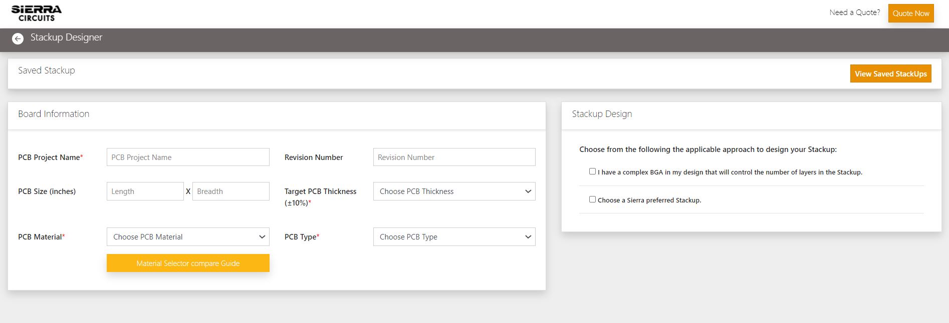
PCB stack-ups represent the construction of multilayer circuit boards. They provide crucial information such as trace width, copper weight, dielectric thickness, and spacing.
Our Stackup Designer provides precise options for cost-optimized build-up structures. It also comes with an impedance calculator that can be used to calculate the desired impedance, as well as trace and space values for any signal layer.

Fill out your board information such as project name, revision number, PCB size (length and width), target board thickness, material, and board type. After providing the board info you will have to choose one of the following approaches:
- I have a complex BGA in my design that will control the number of layers in the stack-up
- Choose a Sierra preferred stack-up
Choose the second option if you’re aware of the number of signal layers and the combination (signal/plane) in your board. Once the necessary input is given, click on stack-up generator to view stack-up options for your HDI and standard PCBs.
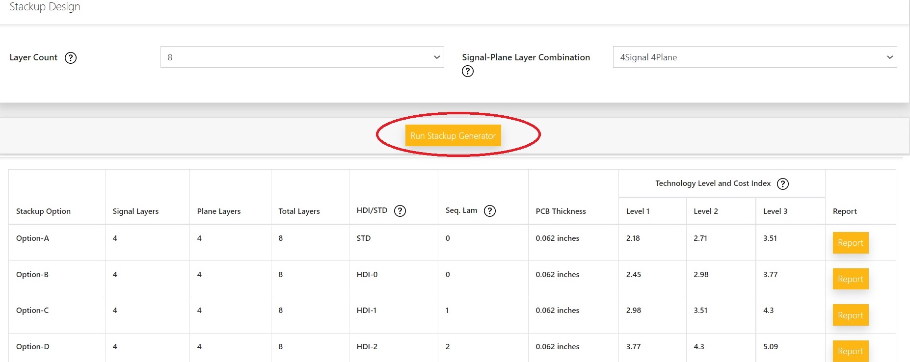
To view the detailed stack-up, click on report.
Here, there is a provision to edit the board parameters without going back to the previous page. Please remember to hit generate custom stack-up if you make any changes to the input.
If your design has controlled impedance traces, you can use the built-in impedance calculator. This calculator allows you to add the impedance model and compute the desired trace geometry and spacing for a target impedance. In addition to this, the tool provides technology parameters and cost index that defines the drill size, pad size, and trace width parameters that can be used in your design.
Impedance Calculator
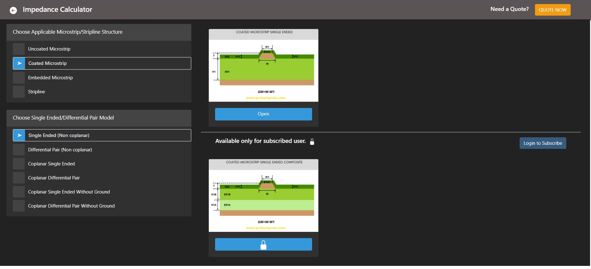
Our Impedance Calculator employs a 2D numerical solution of Maxwell’s equations for PCB transmission lines. It provides accurate and suitable impedance values for circuit board manufacture. This calculator also estimates trace parameters such as capacitance, inductance, propagation delay per unit length, and the effective dielectric constant of the structure.

The tool features various microstrip and stripline structures for single-ended and differential models. Choose the right impedance calculator mode based on the geometry of the signal layer and the relevant reference plane(s).
Here, we’ll have a look at the functionality of the coated microstrip single-ended impedance calculator.
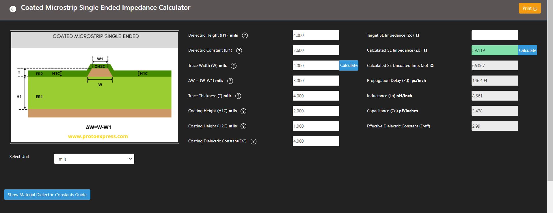
To calculate the single-ended impedance for a specific trace width, you will have to input the dielectric height, dielectric constants, trace width, delta w(ΔW), trace thickness, and coating heights.
Note: You can select the unit (mils/inches/mm/um/cm) of these parameters using the dropdown at the bottom left. Also, if you require any assistance with dielectric constant click on Show Material Dielectric Constant Guide. This shows the dielectric constant of various commonly used materials.
After providing all the necessary data, hit calculate besides the calculated SE impedance field.
The calculator now displays the values of the following parameters:
- Calculated single-ended coated and uncoated impedance
- Propagation delay
- Inductance
- Capacitance
- Effective dielectric constant
If you would like to calculate the trace-width for a target impedance, you’ll have to key in dielectric height, dielectric constants, ΔW, trace thickness, coating heights, and target impedance. Now, hit Calculate besides trace-width field to view the optimum trace-width for the given impedance.
Most of the online impedance calculators may not provide you with precise data as they’re based on empirical formulas and don’t account for the trapezoidal shape of the trace or the effect of numerous dielectric materials. Sierra Circuits’ Impedance Calculator considers these paramount factors to impart the most accurate data.

Controlled Impedance Design Guide
6 Chapters - 56 Pages - 60 Minute ReadWhat's Inside:
- Understanding why controlled impedance is necessary
- Stack-up design guidelines
- How to design for impedance
- Common mistakes to avoid
Download Now
Material Selector
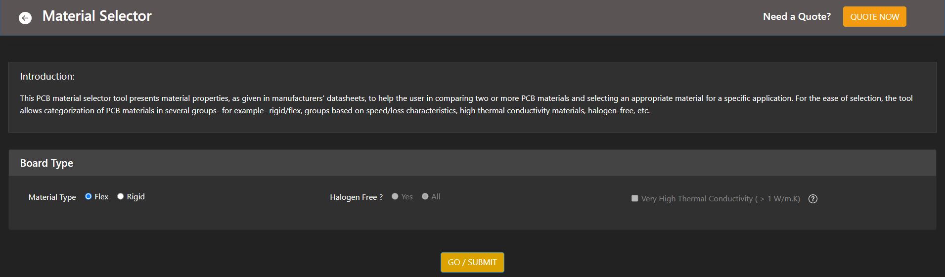
Material selection is the initial step in your PCB design process. The dielectric material you choose for your design is critical since it can affect the board’s overall performance.
To help you to determine the dielectric(s) that best suits your design, we have developed a Material Selector tool. Using HDI standard board tool, you can compare the properties of board materials that fit your application. It has more than 50 rigid and 10 flexible materials.

First, you will have to select the board type (flex/rigid). If you select flex material type and click on Go/Submit, the tool directly lists the available flexible materials in the database as shown below.
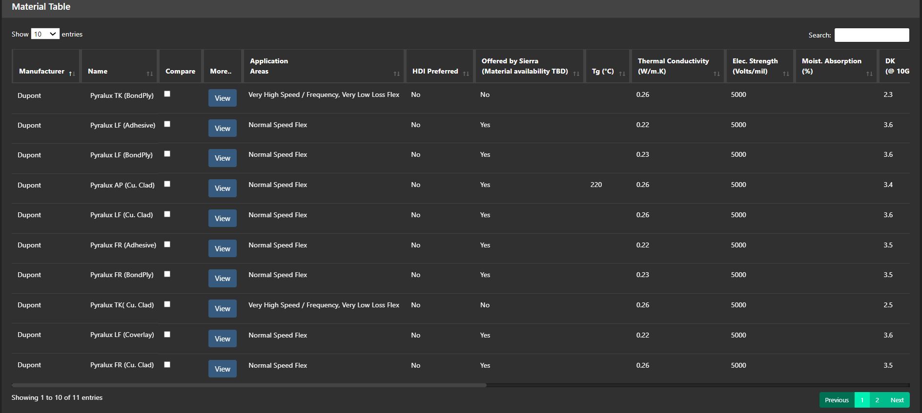
By clicking the “View” button, you can view the properties of that particular material. To compare the properties, select the materials that you would like to analyze and hit “Compare”. A new window pops up comparing the properties of the chosen materials.
Note: You can compare up to 7 materials at a time.
If you select rigid material type, you can define the various electrical, thermal, chemical, and mechanical properties of the dielectric you’re looking for.
You can also narrow down your search if you’re specifically looking for halogen-free and very high thermal conductivity material by selecting the respective radio buttons.
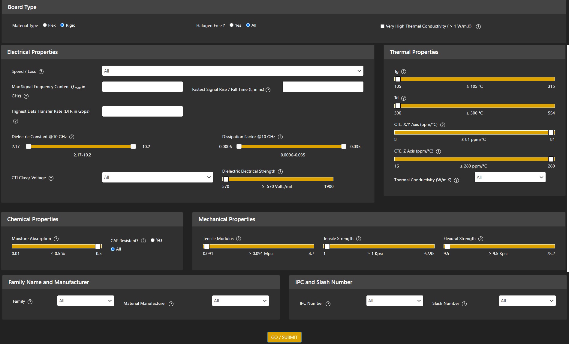
The below table lists the properties that you can define using our Material Selector.
| Category | Properties |
|---|---|
| Electrical | Category of speed and loss, maximum signal frequency, highest data transfer rate, dielectric constant, dissipation factor, CTI, and dielectric electrical strength. |
| Thermal | Glass transition temperature, decomposition temperature, CTE and thermal conductivity. |
| Chemical | Moisture absorption and CAF resistant. |
| Mechanical | Tensile modulus, tensile strength and flexural strength. |
In addition to the parameters mentioned in the table, you can also look for the materials specific to family name/manufacturer and IPC/slash numbers.
Once all the requirements are defined, click on Go/Submit to view the list of materials that are suitable to your design.
If you do not define any of the properties and hit Go/Submit, the tool displays all the rigid materials that are available in the database.
Simplification of the design complexity is one of the primary advantages of using these PCB design tools. These HDI standard board tools consider all the industry design standards which enable your HDI or standard board to be fabricated right the first time. In addition to this, they also help you in the reduction of overall cost and lead time. Check out all our Designer’s tools to make your PCB design process quick and efficient. Let us know in the comment section if you require any help in using these tools.


