Speak to an Account Manager
![]() +1 (800) 763-7503
+1 (800) 763-7503
Related Categories — PCB Assembly » PCB Design » PCB Layout
9 Drawing Requirements for Flex PCBs
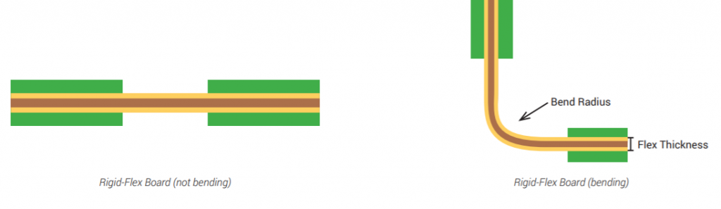
To successfully design a flexible PCB, it is important for the designers to have a basic understanding of the flex drawing requirements.
Flex PCBs
14 Tips For PCB Design For Assembly
Designing with PCB assembly in mind is one of the most important and frequently misunderstood elements. This series is ... more »
PCB Assembly
Role of PCB Trace Current Capacity in Design
The restrictions posed by the PCB trace current capacity are critically important when it comes to PCB design. ... more »
PCB Design
9 Drawing Requirements for Flex PCBs
To successfully design a flexible PCB, it is important for the designers to have a basic understanding of ... more »
Flex PCBs
14 Tips For PCB Design For Assembly
Designing with PCB assembly in mind is one of the most important and frequently misunderstood elements. This series is ... more »
PCB Assembly
Role of PCB Trace Current Capacity in Design
The restrictions posed by the PCB trace current capacity are critically important when it comes to PCB design. ... more »
PCB Design
How to Avoid Crosstalk in HDI Substrates?
Miniaturization of the copper features in electronic circuits results from placing interconnections closely with a high packing density. ... more »
HDI / Blind & Buried Vias
7 Considerations for PCB Power Supply Design
Have you ever thought about how power is being transferred within complex PCBs? Yes, it is a challenging ... more »
PCB Design
The Effects of High-Speed Signals in a PCB Design
The designers are constantly challenged to improve the performance of an electronic product. At the same time, the ... more »
High Speed
9 Factors that Lead to Signal Integrity Issues in a PCB
Avoiding signal integrity issues in a PCB is an extremely complex task for designers. It requires a deep ... more »
Controlled Impedance
How to Export Gerber and Production Files in Altium Designer
In this tutorial, we will show you how to export Gerber and other production files in Altium Designer.
PCB Design
The Advantages of HDI PCBs and their Applications
The digital world is getting complex hour by hour whereas the hardware associated with it is getting drastically ... more »
HDI / Blind & Buried Vias


Fabrication, Procurement, & Assembly. PCBs fully assembled in as fast as 5 days.
- Bundled together in an entirely-online process
- Reviewed and tested by Engineers
- DFA & DFM Checks on every order
- Shipped from Silicon Valley in as fast as 5 days

Fabrication. Procurement & Assembly optional. Flexible and transparent for advanced creators.
- Rigid PCBs, built to IPC-6012 Class 2 Specs
- 2 mil (0.002″) trace / space
- DFM Checks on every order
- 24-hour turn-times available

Complex technology, with a dedicated CAM Engineer. Stack-up assistance included.
- Complex PCB requirements
- Mil-Spec & Class 3 with HDI Features
- Blind & Buried Vias
- Flex & Rigid-Flex boards