Related Categories — HDI / Blind & Buried Vias » PCB Design
How to Achieve a Robust PCB Design Workflow for Signal Integrity?
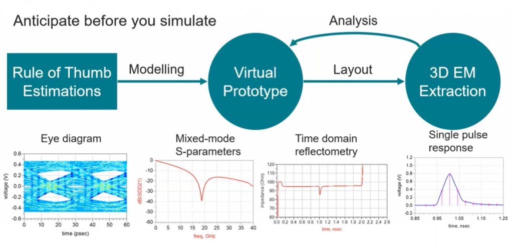
Signal Integrity (SI) signifies the signal’s ability to propagate along PCB traces without distortion. Signal integrity is about the quality of the signal passing through a transmission line. In this article, Tim Wang Lee acknowledges some of the designers’ pain points regarding robust PCB design workflow and signal integrity.
PCB Design
Gerber, ODB++ and Other PCB Design Files Required by a Manufacturer
PCB is the backbone of all major electronic devices and is also responsible for making devices compact and ... more »
PCB Design
Understanding Signal Integrity in PCBs
When a signal is transmitted, the received signal will always be distorted as a consequence of impedance and ... more »
PCB Design
How to Achieve a Robust PCB Design Workflow for Signal Integrity?
Signal Integrity (SI) signifies the signal’s ability to propagate along PCB traces without distortion. Signal integrity is about ... more »
PCB Design
Gerber, ODB++ and Other PCB Design Files Required by a Manufacturer
PCB is the backbone of all major electronic devices and is also responsible for making devices compact and ... more »
PCB Design
Understanding Signal Integrity in PCBs
When a signal is transmitted, the received signal will always be distorted as a consequence of impedance and ... more »
PCB Design
What is Power Integrity and Power Distribution Network?
Power integrity is one of the mind-boggling subjects when it comes to PCB designing. In this blog, we ... more »
PCB Design
How to Choose PCB Laminates and Materials for Fabrication
PCB material selection is the first step in your PCB design process. Selecting the right materials for your ... more »
PCB Design
How to Use Via-in-Pad for PCB Design and Manufacturing
Multi-layered printed circuit board design requires a means to establish connections between various layers. This is done using ... more »
PCB Design
Becoming a PCB Design Master: Designing for Layout
Proper layout design is vital for printed circuit board success, making it essential for designers to understand best ... more »
PCB Design
How To Limit Impedance Discontinuity and Signal Reflection in PCB Transmission Lines
We previously quickly discussed signal reflection in our PCB transmission line article. This is an in-depth article about ... more »
PCB Design
How to breakout a .4mm BGA
One thing PCB designers will all agree on is that to breakout a BGA, you need precision and ... more »
HDI / Blind & Buried Vias
Fabrication, Procurement, & Assembly. PCBs fully assembled in as fast as 5 days.
- Bundled together in an entirely-online process
- Reviewed and tested by Engineers
- DFA & DFM Checks on every order
- Shipped from Silicon Valley in as fast as 5 days
Fabrication. Procurement & Assembly optional. Flexible and transparent for advanced creators.
- Rigid PCBs, built to IPC-6012 Class 2 Specs
- 2 mil (0.002″) trace / space
- DFM Checks on every order
- 24-hour turn-times available
Complex technology, with a dedicated CAM Engineer. Stack-up assistance included.
- Complex PCB requirements
- Mil-Spec & Class 3 with HDI Features
- Blind & Buried Vias
- Flex & Rigid-Flex boards


