


Contents

On-demand webinar
How Good is My Shield? An Introduction to Transfer Impedance and Shielding Effectiveness
by Karen Burnham
Transient spikes in PCBs can lead to signal integrity issues and component malfunctions. Proper decoupling or bypass capacitor placement is required to stabilize voltage levels and suppress electrical noise.
In this article, you will learn how bypass capacitors control voltage fluctuations in circuit boards and decoupling strategies for boards without power planes, with closely spaced planes, and with broadly spaced planes.
Highlights:
- Suitable decap placement ensures stable voltage levels and minimizes high-frequency noise, preventing power integrity issues and signal degradation in PCBs.
- Capacitors should be placed as close as possible to IC power pins, with minimal loop inductance, to meet the demands of modern high-speed circuits and avoid EMC compliance failures.
- Placement techniques, such as using multiple capacitors of the same value, implementing via-in-pad technology for BGAs, and prioritizing low-value capacitors near power pins, ensure reliable performance and signal integrity.
Concept of decoupling in PCBs
Decoupling capacitors isolate AC signal components from the DC power supply and ensure that components receive a stable voltage. These capacitors also help suppress transient spikes and reduce electromagnetic interference (EMI), making them critical for modern high-speed, high-density PCB layouts.
Effective decoupling depends upon the capacitor type, its value, and placement on the board.
To understand the purpose of decaps, see what is the use of a decoupling capacitor.
How decoupling capacitors control voltage fluctuations in PCBs

When an active device (microcontroller or FPGA) suddenly switches states, it momentarily draws a sudden surge of current. This transient current causes a voltage drop across the connecting traces due to its inherent impedance.
Even a very low resistance or inductance in the power trace can result in significant voltage dips at high frequencies.

These voltage drops don’t just impact the device that switched. They can propagate across the entire PDN (power distribution network), affecting the operation of other nearby components. Some circuits may reset, malfunction, or produce timing errors if the voltage dips too low. Additionally, these rapid fluctuations can radiate as EMI, which may cause the device to fail EMC tests.
Here’s how it works:
- The capacitor is connected in parallel with the power and ground pins of the device. Under normal, steady-state conditions, the capacitor charges up to the supply voltage.
- When the active device suddenly demands a large amount of current (during a switching event, for example), the decaps can quickly discharge and supply this transient current locally. Because the capacitor is placed very close to the device, the path for this transient current is short, minimizing the detrimental effects of trace inductance.
- By providing this immediate burst of current, the capacitor prevents the voltage at the device’s power pins from dropping significantly. It effectively decouples the high-frequency current demands of the local device from the main power distribution network.
- Once the transient current demand subsides, the main power supply has time to react and recharge the bypass capacitor.
Download our eBook to learn how to design high-speed PCBs with signal integrity.

High-Speed PCB Design Guide
8 Chapters - 115 Pages - 150 Minute ReadWhat's Inside:
- Explanations of signal integrity issues
- Understanding transmission lines and controlled impedance
- Selection process of high-speed PCB materials
- High-speed layout guidelines
Download Now
3 challenges PCB designers face when placing decoupling capacitors
In our recent webinar, designing for ultra-linear RF: what matters beyond the IC, we surveyed PCB designers to understand the challenges they face with decoupling capacitor placement.

The results revealed that:
- 42.9% of respondents struggled to pick the right capacitor values and types to go along with different ICs.
- 35.7% faced difficulties placing decaps efficiently.
- 21.4% found it challenging to strike a balance between capacitor count and space constraints.
In the following sections, you’ll learn strategies to overcome these obstacles.
How to choose the right capacitors for your ICs
The choice of the decaps depends on the IC’s operating frequency, transient current demands, circuit type (analog, digital, or mixed-signal), switching speed, and the target impedance of your PDN.
Stick to these guidelines when picking a capacitor:
- Check the IC datasheet for recommended decoupling capacitor values, self-resonant frequency (SRF), and transient current requirements.
- For high-speed digital ICs (e.g., FPGAs, CPUs, microprocessors), use a combination of 0.01 µF to 0.1 µF capacitors. Their low parasitic inductance allows fast response to instantaneous current demands.
- Add 10 µF or higher bulk capacitors to stabilize the power rail and handle slower transient currents. This combination ensures coverage across both high-frequency transients and low-frequency stability.
- For analog or mixed-signal ICs, always refer to the datasheet, since these devices are often more sensitive to noise and may require specific capacitance ranges. Typical designs use 1 µF to 10 µF capacitors for low-frequency stabilization.
- Use ceramic capacitors for high-frequency decoupling because of their low ESR/ESL. Choose electrolytic or tantalum capacitors for bulk decoupling and low-frequency stability. Prioritize smaller packages (0201, 0402) for low-power ICs to minimize inductance.
- Choose capacitors with an SRF near the noise frequency. Example: RF ICs at ~1 GHz may need 1 nF to 10 nF ceramics with low ESL.
- Select capacitors with a voltage rating higher than the maximum circuit voltage and ensure they can handle your circuit’s operating temperature range.
By matching capacitor values to the IC’s requirements, you can effectively suppress voltage fluctuations and maintain signal integrity.

Fill out the form:
How to strike a balance between capacitor count and board space
In dense PCB designs, such as those with BGAs or high-speed processors, balancing the number of decoupling capacitors with available board space is a common challenge.
Here’s how you can reduce the capacitor count:
- Prioritize decoupling for high-speed processors, clock generators, and noise-sensitive analog circuits. Focus on ICs with the highest current consumption and fastest switching rates. Simple logic gates and low-power ICs can share bulk decoupling capacitors.
- Use via-in-pad to maximize the number of capacitors you can place under BGAs. This reduces the space occupied by footprints and minimizes inductance.
- Employ low-value, high-frequency capacitors near the IC, and use bulk capacitors near voltage entry points (e.g., power supplies or converters).
- Opt for compact ceramic capacitors (e.g., 0402 or 0603) with low ESL to fit more capacitors in tight spaces. These smaller packages maintain performance while reducing footprint.
What are the decoupling capacitor placement strategies for different power plane configurations?
Maintaining low impedance on the power bus across a specific range of frequencies is one of the main goals when designing a PDN. This ensures stable voltage delivery and signal integrity during rapid current demands.
When digital devices (such as CPUs, FPGAs, etc.) switch states, they require higher current. The amount of current drawn is directly influenced by the rise and fall times of the signal. Shorter rise time signals draw higher current.
As a result, maintaining low impedance (at higher frequencies) in power traces is necessary to support rapid transitions without causing voltage drops or introducing noise.
The frequency range depends on the speed of the signals in your active components:
- The lower end is typically the main clock frequency.
- The upper end is defined by the rise time of your fastest switching signals.
For example:
If a signal has a rise time of 0.5 nanoseconds, the upper frequency is: BW = 0.35/Tr
= 0.35/ 0.5 ns = 0.7 GHz
For a rise time of 250 picoseconds, the upper frequency becomes: 0.35 / 0.25ns = 1.4 GHz
In high-speed systems (e.g., gigabit transceivers), rise times can be as low as 50 picoseconds, pushing the upper frequency to 7 GHz and beyond.
Maintaining a low impedance across this frequency range is crucial because it allows the PDN to supply instantaneous current when ICs switch. Failing to do so can result in voltage ripple, timing errors, and degraded power integrity.
The acceptable impedance level is calculated using the formula below:
Target impedance = maximum allowable voltage ripple / maximum instantaneous current
Steve Sandler, Power Integrity Expert, Picotest, explained, “To calculate the exact capacitance needed, use the formula, C = L / (R²), where L is the inductance of the power plane, and R is the target impedance. The capacitor’s ESR should be close to the target impedance to maintain a flat impedance profile. However, it’s challenging to balance low inductance with the right ESR, and paralleling capacitors might lower ESR too much, causing new resonances.”
For more, read the full interview: Steve Sanlder’s on power integrity in PDN design and high-speed simulations.
As a PCB designer, you need to implement a combination of capacitors and properly designed power and ground planes to achieve the low impedance across the required frequency range.
These elements work together to supply fast transient current and maintain a stable voltage at the device pins.
PCBs can be segregated into three categories for power bus decoupling:
- Boards that do not have power planes
- Boards with closely spaced power planes
- Boards with broadly spaced power planes
Placing decaps on boards without power planes
Follow these techniques if your design does not have power planes:
- Place at least one local bypass capacitor for each active device on the board between the voltage and ground pins of the active device, and keep it near the IC pin.
- Use capacitors with nominal values: 0.001 µF, 0.01 µF, 0.1 µF, or 0.047 µF.
- Place at least one bulk capacitor (10 µF) for each voltage distribution on the board.
- Make sure that the area of the loop formed by the capacitor connection is minimal.

Illustration of a local decoupling capacitor mounted near the IC’s power pin to ensure a small loop area between ground and power pins (top view). - Place bulk decaps near the voltage entry points (power supplies, output convertor, load). The bulk capacitance should be 2 to 10 times the local decoupling capacitance on the same voltage bus, though the exact value should be based on design needs and validated through experimentation.

Bulk decoupling capacitor placement on a power distribution network. - Place two local capacitors having the same nominal value rather than placing one capacitor with an equivalent capacitance. The reason is that two capacitors have an effective series inductance (ESL) less than a single capacitor, and this improves high-frequency performance due to parallel connections.

Implementing decaps on PCBs with closely spaced power planes
Densely packed power planes (separated by 10 mil (0.25 mm) or less) are common in boards with 8, 10, or 14 layers. Their proximity creates high inter-plane capacitance and significantly lowers inductance compared to capacitor connections.
As a result, these planes provide the primary low-impedance path for high-frequency current during fast signal transitions, supplying energy more efficiently to switching ICs.
The exact location of the local decaps relative to the IC power and ground pins is less critical, in contrast to boards without planes or with widely spaced planes. They don’t have to be right next to or directly under the IC in the same way. The energy will mainly be delivered through the low-inductance planes.
The capacitors need to be close enough to the IC to effectively recharge the planes and handle slightly lower frequencies. Close enough relates to how far energy can travel through the planes during the signal rise time. This creates an effective energy circle around the IC, where capacitors placed within this area are beneficial. The faster the signal rise time, the smaller this effective circle.
Follow these guidelines if your board has closely spaced power planes:
- Select capacitors with values optimized for the transient current requirements of the active device and the target impedance of the PDN. Typically 0.01 µF to 0.1 µF for high-frequency decoupling. Larger capacitors (e.g., 10 µF or 100 µF) are better suited for handling low-frequency transients and stabilizing the power supply. Use multiple identical capacitors in parallel to avoid resonance peaks and ensure broadband performance.
- Use multiple decaps of the same value near the power supply. If not possible, add the lowest-value capacitor closest to the power supply, as shown in the image below.

Multiple decoupling capacitors in parallel with an active device’s power supply. Atar Mittal, General Manager at Sierra Circuits, explains, “When you have multiple capacitors with different values and resonant frequencies in a circuit, there is a possibility of generating resonance peaks in the frequency response of the circuit. These peaks can lead to impedance discontinuities at specific frequencies. To avoid this, you can incorporate multiple capacitors of the same value near the power supply.”
- Use multiple decaps to reduce the effective connection inductance. The number of capacitors is inversely proportional to the effective connection inductance. For high-speed circuit boards, place several local decoupling capacitors around each active device to compensate for the parasitic inductance of the mounting structure. Keep the current loop area small by optimizing the capacitor body placement, mounting pads, traces, and vias.
- Leverage power planes for high-frequency energy delivery. Closely spaced power planes act as the primary energy reservoir for the fastest transient currents in high-speed circuits. These planes deliver high-speed energy more efficiently than discrete capacitors. In this setup, bypass capacitors mainly support lower-frequency transients and help replenish the planes after each burst of current.
- Place capacitors within an effective region around the IC rather than directly at each power pin. Because the planes handle the highest-frequency transients, precise placement is less critical. Instead, ensure capacitors are located within an area around the IC where energy can reach during the signal’s rise time.
- Avoid routing traces between the capacitor pad and the via. Instead, place vias within or immediately adjacent to the capacitor pads. Any trace length between the capacitor and via/IC pin adds inductance, which degrades high-frequency performance. If traces are unavoidable, make them as short and wide as possible.
- Mount local capacitors as close as possible to the power and ground planes. Connection inductance increases with vertical distance from the planes, so minimizing this spacing helps maintain low impedance and better high-frequency decoupling.
- Minimize inductance in capacitor-to-plane connections, even if horizontal clearance is relaxed. While closely spaced planes reduce the criticality of capacitor position, low-inductance vertical connections are still essential for capacitors to remain effective across their intended frequency range.
- Use capacitors with a higher self-resonant frequency (SRF) (2 to 3 times the operating frequency) to filter out high-frequency noise effectively.
- Use polygons to connect bulk capacitors to power/ground planes.
Download our eBook to learn how to design PCBs with controlled impedance.

Controlled Impedance Design Guide
6 Chapters - 56 Pages - 60 Minute ReadWhat's Inside:
- Understanding why controlled impedance is necessary
- Stack-up design guidelines
- How to design for impedance
- Common mistakes to avoid
Download Now
Incorporating capacitors on boards with widely spaced power planes
In a typical four-layer board, the PCB stack-ups are often 62 mil (1.6 mm) thick, with a clearance of about 40 mil (1 mm) between ground and power layers. This wide spacing creates a very small inter-plane capacitance, which means the planes contribute very little to high-frequency decoupling.
When planes are far apart, their ability to store energy is minimal, and their impedance becomes much higher. This makes them less effective at delivering power to your ICs, especially during high-speed transitions. To compensate, you need to carefully design how components like vias and capacitors connect to these planes.
Follow these decoupling capacitor placement guidelines if your board has broadly spaced power planes:
- Place vias from the capacitor as close as possible to the IC power and ground pins. Keep the power and ground vias tightly grouped and positioned near the corresponding pins to minimize loop inductance.
Daniel Beeker, Technical Director at NXP Semiconductors, says, “While placing the capacitor, employ the 20th wavelength of transistor switching speed. Implement the capacitor as near as possible to the IC pin to limit the propagation time. When you consider a one-nanosecond switching event, place the capacitor at half an inch of distance for a good power supply within the 20th wavelength. Usually, capacitors are attached to the bottom side of the board for BGAs. For QFPs and similar packages, it is implemented across the pair of leads.”
- Connect decoupling capacitors to the IC pin that is linked to the more distant power or ground plane. For example, on a 4-layer board where the IC is on layer 1 and the Vcc and GND planes are on layers 2 and 3, place the decoupling capacitor near the ground pin if the ground plane is farther from the IC.

A decoupling capacitor is mounted near the IC’s ground pin, as the ground plane is distant from the IC. - Use opposite polarity vias in pairs. Position one via to power and one to ground side-by-side, near the IC power pins, to create the lowest impedance path.
- Mount decaps on the same side of the board as the IC and very close to the IC pins. Avoid placing capacitors on the opposite side (exception for BGAs), as this significantly increases the inductance of the power delivery path and degrades performance.
- Avoid traces between capacitor pads and vias. Place vias directly within or immediately adjacent to the mounting pads to reduce inductive effects.
- Use bulk decoupling capacitors (10–100 µF) for low-frequency transients. Select their value based on the equation: C = I × (Δt / ΔV), where I is the transient current, Δt is the transient duration, and ΔV is the allowed voltage ripple.
- Prioritize local capacitors for high-frequency decoupling. Their effectiveness is more dependent on low connection inductance than on nominal capacitance.
- Locate local decoupling capacitors as close as possible to the IC. Ideally, they should share the same via. Avoid inserting traces between the capacitor pad and via.
- Never use vias between the decoupling capacitor and the IC when placed on opposite board sides. Always mount local capacitors on the same side as the IC to reduce inductance.
- Avoid trace routing on decoupling capacitors. Place vias next to the BGA mounting pads and keep power and ground vias as close together as possible to reduce the connection inductance.

Place ground and power vias next to the BGA mounting pads to reduce the connection inductance.
To learn how to identify signal integrity issues using an eye diagram, see analyzing eye diagrams for signal integrity in high-speed PCBs.
Where should you implement decoupling capacitors for signal and power integrity?
In this section, you will learn practical techniques for placing decaps to improve power delivery and signal stability in your PCB layout. These tips focus on optimizing loop inductance, minimizing noise, and maintaining impedance for high-speed and mixed-signal designs.
6 tips for effective decoupling capacitor layout
- Ensure each power supply rail has its own set of decaps, as different power rails may have different current demands and impedance requirements.
- Add multiple vias to connect the decoupling capacitors with the power and ground planes. This minimizes the loop area and the via inductance.
- Place the capacitors directly on the power plane through short vias to avoid trace stubs.
- Connect the component pin to the capacitor first and then to the via. This ensures a short current path for noise filtering and maintains low impedance.

Ideal decoupling capacitor placement: connect the capacitor to the component pin, then to the via - Filter out high-frequency noise by connecting the capacitor in parallel with a resistor. This forms a low-pass filter, allowing DC and low-frequency signals to pass while attenuating high-frequency components.
- In certain cases, capacitors can be connected in series with I/O signal traces to block DC or low-frequency components while allowing high-frequency signals to pass. This is known as AC coupling and is commonly used in communication interfaces like Ethernet or HDMI.
At Sierra Circuits, we can build PCBs with ±5% impedance tolerance. We add impedance test coupons to each panel and validate the impedance to ensure it matches your requirements. These test coupons replicate the trace structure and layer stack-up of the actual PCB.

See our controlled impedance capabilities to learn more.
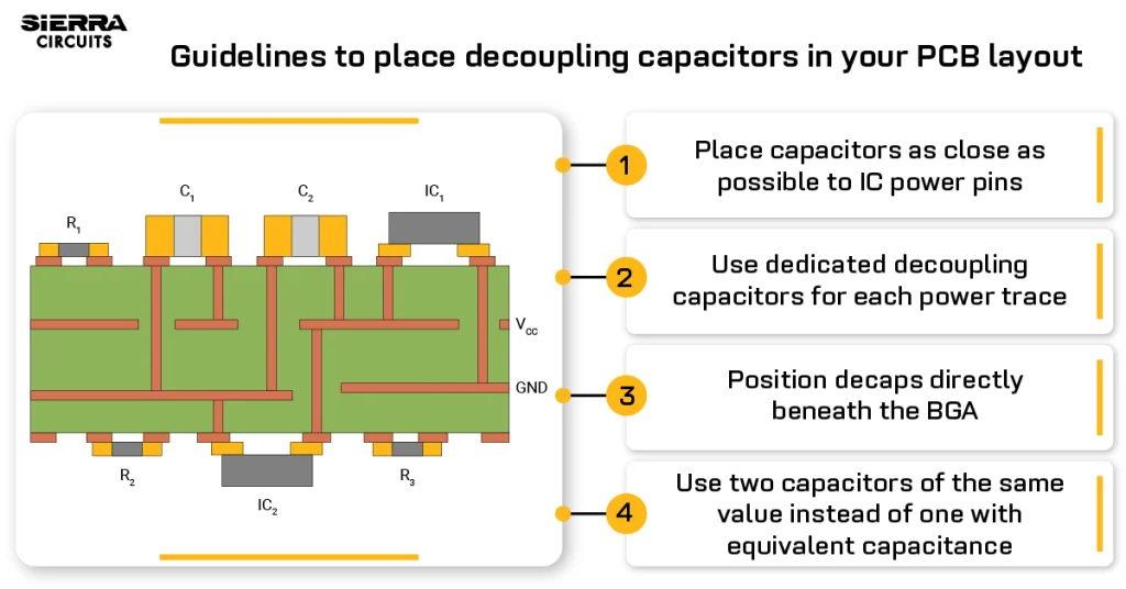
8 guidelines for incorporating bypass capacitors on PCBs with BGAs
- Place decoupling capacitors directly under the BGA to shorten the distance between power pins and capacitors.

Bulk and local decoupling capacitor placement on a BGA. - Have capacitors between two BGA rows when space permits to reduce loop inductance.
- Position the capacitors on the opposite side of the board across the periphery of the BGA.

Decoupling capacitor placement on the opposite side of a BGA. - Align the capacitors so that the BGA-fanout vias can be used to connect the decaps. This orientation minimizes inductance and saves space for signal routing.
- Implement via-in-pad technology to connect capacitors directly to BGA power pins, ensuring a low-inductance path for power delivery.
- Share vias between adjacent power or ground balls to reduce via count and free up space under the BGA for capacitors. This allows decaps to fit directly underneath the BGA, reducing inductance compared to placement outside the footprint. Avoid sharing more than two balls per via to maintain low impedance.
- Place capacitors inside the BGA matrix only when existing fanout vias are available. Adding extra vias in this region can reduce the copper plane area and impact power delivery.
- In BGAs with ground pins at the center and surrounding power rows, reroute outer ground vias to inner rows. This opens routing channels for placing more capacitors close to the power pins on the bottom layer.
Key takeaways:
- Use multiple capacitors of the same value in parallel to cover a broad frequency range and avoid resonance peaks in the PDN.
- Prioritize low-value capacitors near power pins when using multiple capacitors of different values for the same power pin, as they respond faster to high-frequency demands.
- Position bulk decoupling capacitors near voltage entry points, such as power supplies or converters, to stabilize the overall power bus.
- Minimize loop area by placing vias adjacent to capacitor mounting pads and connecting them directly to power and ground planes to reduce inductance.
- Avoid using traces between capacitors and vias. Use short, wide traces only if necessary to maintain low impedance.
- Ensure each power supply rail has its own set of decoupling capacitors to meet specific current demands and impedance requirements.
In high-speed and high-density PCB designs, proper decoupling capacitor placement is critical as it directly impacts the power integrity. Thoughtfully positioned decaps ensure stable power delivery, suppress high-frequency noise, and protect sensitive components from voltage fluctuations. By following best practices in placement and selection, you can significantly enhance signal integrity, minimize EMI issues, and build more reliable electronic systems.
Have queries regarding decoupling capacitor placement? Post them on our community, SierraConnect. Our design experts will answer them.

About Mohamed Faheemuddin : Mohamed Faheemuddin is a mechanical engineer. His passion for electronics drew him to the PCB industry. With an experience of over 3 years in the PCB industry, he specializes in developing articles for engineers and hardware designers.


Start the discussion at sierraconnect.protoexpress.com