Get an instant online quote for manufacturing and assembly of standard PCBs. Sierra Circuits provides flexible and transparent pricing for fast and easy ordering.
Online Ordering Process
What are the steps in ordering PCBs online?
- Go to the instant web quote screen and fill in your PCB specs.
- Option to include parameters for assembly and to upload your BOM.
- Complete the check-out process and upload your zipped Gerber files.
After you place your order, track your order online. Your design will be reviewed and you will be contacted if there are any discrepancies. Be available to answer questions, respond to suggestions from the review of your files by our technical support center. Even if your design doesn’t meet these specs, you will find our matrix has a place to upload your file for a custom quote. Do so and we’ll email you a custom quote quickly!
Required Files to Support Fabrication
What files are required to generate an online quote for PCB fabrication?
For orders that include PCB fabrication:
- The following files are needed as part of a zip package when you place an order: Gerber files using English units in RS-274X format or ODB++ format. (Note: 274D format is not accepted)
- Fabrication print in Gerber format, showing the board outline with drill pattern and sizes.
- Exellon drill file in ASCII format with the following parameters:
- Units = Inch
- Tool Units = Inch
- Coordinate = Absolute
- Zeros omitted = Trailing
- Number format = 2.4
- ASCII text file called Readme.txt with the following critical information:
- All relevant details about the board, including thickness.
- Listing of all file names and descriptions (e.g. top copper, top solder mask, bottom solder mask, etc).
- Layer stack-up sequence
- Board outline
- We STRONGLY PREFER that board outline should be in the Gerbers– it could be on any of the Gerber layers or on its own separate layer.
- If that is not possible, our second preference would be to have the outline in the fabrication drawing with dimensions clearly shown.
- Any other way of representing the outline would not be acceptable and your order may go on-hold.
Required Files to Support Assembly
What files are required to generate an online quote for assembly?
For orders that include assembly (optional):
- Upload your BOM file online during the quoting process and component pricing will happen instantly based on the data included in your BOM. Follow the format in this sample BOM.
- When you place an order you will upload the zip file with gerbers in it. In that zip file, we will also expect XY Data and Assembly Drawing (see sample XYRS file here).
- If you are placing a turnkey or partial-turnkey assembly order, we will not need a BOM file with your zipped Gerber files, since we will only use BOM data from you already loaded online during the quoting process.
- If you are placing a fully consigned assembly order, then include a BOM file in addition to your zipped Gerber files.
How are the Kapton tapes specified? Can it be specified in the assembly drawing or as special instructions when placing an order?
The Kapton tape specifications must be mentioned in the assembly drawing. If the design is complex, then it would be better to approach someone in the assembly facility. On the board side, the solder mask should be specified as LDI or LPI so that accurate masking can be done.
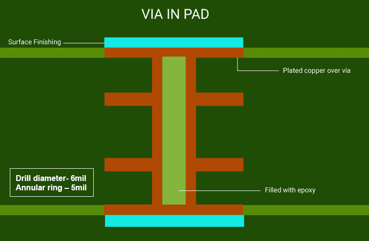
Via-in-Pad features
What if my design has Via-in-Pad features?
If your boards have via-in-pad features on component pads, we put the PCBs through a process of via-filling to ensure good solderability. This is the best practice for board fabrication (regardless of which company assembles the boards.) We specifically ask in the online system if your design has via-in-pad features on component pads; if so, the online system quotes it appropriately. If you indicate No for via-in-pad in the online quote but during our DFM process we do find such features, please understand that this may add to your price and lead time. A customer service team member will contact you accordingly.
PCB Fabrication
What is the best stack-up plan in terms of core and prepreg?
You can request a preliminary stack-up plan as a baseline of your design when you decide the schematic and design.
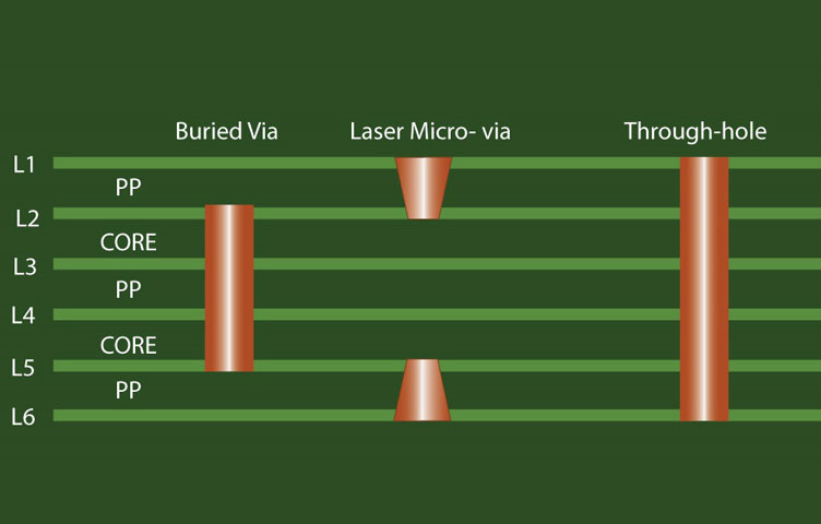
How do I specify core or prepreg in my sequential lamination design?
When a sequential lamination is required (typically for an HDI application with blind and buried vias), it is necessary to specify the maximum number of laminations and the drill details.
You can specify it in the respective EDA tool and then export the stack-up in pdf or excel format.
A sequential lamination PCB board consists of a core on top of which copper foil laminations segregated by prepregs are formed. Sequential lamination is typically implemented when you require blind and buried vias.
Core refers to the glass-reinforced epoxy laminate sheet which has copper on both sides. The copper region is normally etched to form traces. Core is more rigid than prepregs.
Manufacturers stack two cores on both sides of a prepreg and press them at high temperatures. This causes the resin to bond with the adjacent layers and then begins to cure gradually as it cools.
After forming the core out of the first lamination cycle, the mechanically drilled holes are filled with resin. The holes are capped with copper and then the sequential lamination begins.
For the first sequential lamination, a prepreg is placed on both sides of the core followed by a layer of copper foil at the top of the prepreg. This combination is operated under a press and is heated. During the cooling and curing process, the foil binds with the core. This structure is drilled either through laser drilling or mechanical drilling and then etched to add another sequential layer. This process is repeated.
Prepreg is a dielectric material used between a copper and a core or between two cores in a PCB. It binds two layers of a board and acts as a dielectric barrier between two copper layers.
Based on the glass weave, type of resin, and resin content, the dielectric constants will vary in the prepreg and core materials.
Is there any problem if I use non-standard PCB thicknesses?
No issue. Let our engineering team know.
Is this possible to design blind via from 1 to 5 without connecting layer 6?
It is possible by using sequential lamination from 1 to 2, 2 to 3, 3 to 4, and 4 to 5. Because if we use 1 to 5, it is an unbalanced construction. Otherwise, if there is enough space, one battery can be attached on the top of layer 6 before layer 5. Here we will use mechanically drilled 2 to 5 filled with non-conductive material and 1 to 2 above 2 to 5. Sequential lamination is the best approach. Otherwise, direct 1 to 5 connection is unbalanced construction.
Can I use smaller wire bond pads?
Yes, you can get smaller on the wire bond pads. But there are limitations to this. As the boards move and shift, the materials etched on the boards also tend to move and shift. So, if you have too much variation of the true position of that pad, it can lead to a problem since the wire bond machine has a fiducial to register to.
Will there be any effect on the adhesion due to the mask dam?
Generally, no. Unless you use a heavy copper and materials like Roger’s Teflon mask.
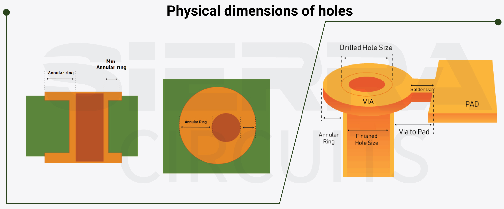
Is it necessary to specify tolerances for vias and plating?
Yes. As a designer, you need to specify the finished hole size you want. If you aren’t worried about the bottom tolerance (meaning, it can go as small as it can), then a fabricator might choose to drill a smaller a hole to provide more annular ring. This can be helpful if it’s a class 3 or a class 2 board.
Should the pads be tape covered during the washing process to avoid contamination?
Yes. To avoid contamination, we use a peelable solder mask that covers the pads until they’re exposed. It can also be taped during assembly.
When should you worry about resin starvation?
If you use heavy copper (>3 oz) in your stack-up, avoid prepregs with very low-resin and high-glass content to reduce the risk of resin starvation.
How many thermal excursions does a PCB have to withstand?
Thermal excursions are associated with the assembly reflow processes. Simple through hole designs may be exposed to the assembly reflow process only once. Designs with Surface Mount components may experience three or four reflow cycles, and additional ones if rework has to be performed. Customers will expect that the printed circuit board should be able to withstand at least four thermal excursions.
Inspection
Is there a way to inspect open soldered joints on BGAs and power supply nets?
Yes. We can inspect the soldered joints using X-ray. If the critical nets need to be tested, they can be added to those test points in the design and the X-ray machine will inspect them.
Does the X-ray machine identify or recognize the gap?
Yes. We can see a hairline crack if there is a gap. For instance, if there are 16 balls that are supposed to touch the same copper plane, whereas only half of them make a proper connection, then the X-ray machine will identify this gap.


