Sierra Circuits has developed easy-to-use tools for designers and electrical engineers at every stage of circuit board development. Try them out and if you have questions, check our PCB design tools FAQs.
Common PCB Design Tools FAQs
Where will I find the PCB design tools offered by Sierra Circuits?
You can access all the design tools on our web homepage under the designer’s tool tab.

Which are the tools present on the Sierra Circuits website?
From stack-up designing to BOM preparation, we have multiple tools to help you expedite the design process, they include:
● PCB Material Selector
● PCB Stackup Designer
● Impedance Calculator and Signal Loss Calculator
● Via Impedance Calculator
● Signal and Plane Layer Estimator
● Via Current Capacity and Temperature Rise Calculator
● Trace Width, Current Capacity, and Temperature Rise Calculator
● Maximum Via Stub Length Calculator
● RLC Resonant Frequency and impedance Calculator
● Bandwidth, Rise Time, and Critical Length Calculator
● Transmission Line Reflection Calculator
● PCB Conductor Spacing and Voltage Calculator
● Better DFM
● BOM Checker
Do I need to install the tools to use them?
Our designer tools are web-based. You don’t have to install them. The tools are compatible with all browsers and operating systems. It can be accessed through mobile devices, tablets, and personal computers.
Are the tools free for all users?
All of the designer’s tools are free to use. You will only require an active Sierra Circuits account to make use of these design applications.
PCB Material Selector
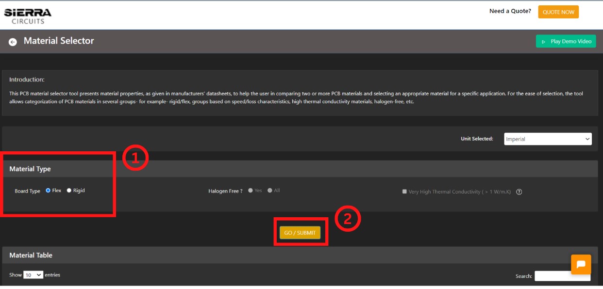
How to search for flex materials?
On the tool page, under the material type section, select the board type as flex and click on Go/Submit. The tool will display all the flexible materials available.
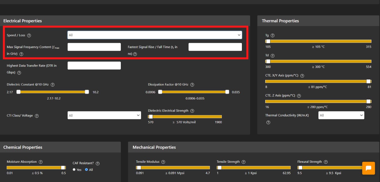
I only know what is the maximum operating frequency of my design. How do I choose the material?
In our tool, under the electrical properties section, we have provided an option to segregate materials based on the different frequency ranges. You can also input the maximum operating frequency and look for the materials that best suit the operating range of your design.
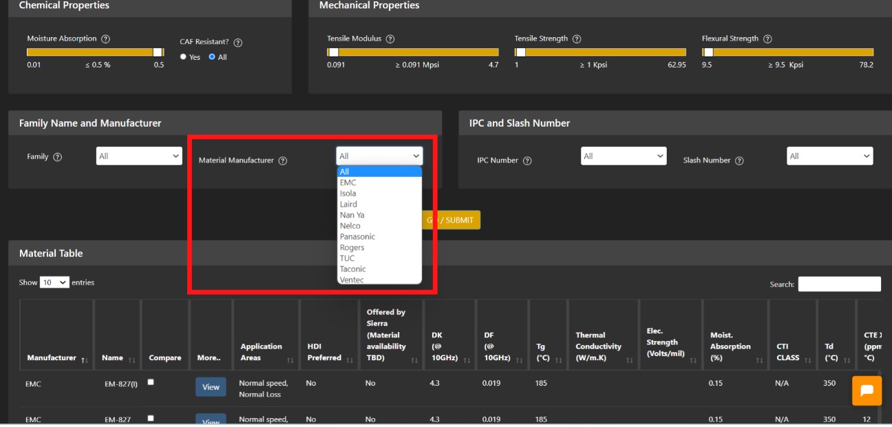
I am looking for material from a specific manufacturer. How can I search for that?
Under the section family name and manufacturer, there is a dropdown to choose your preferred manufacturer.
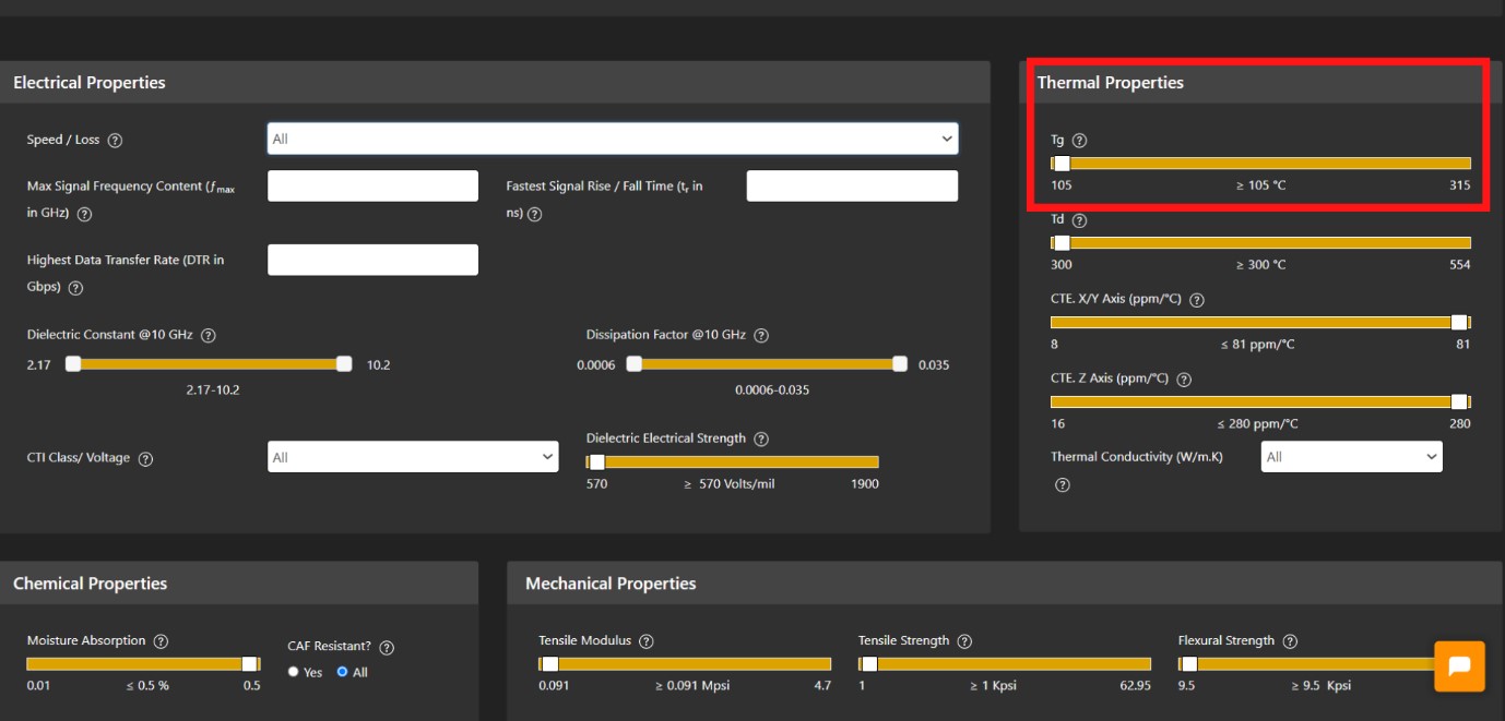
If I want to find material with a specific glass transition temperature. What should I do with other filters?
To segregate materials based on a specific range of glass transition temperatures, adjust the Tg slider under the thermal properties section. Set other parameters to default to avoid them from interfering with the material search.
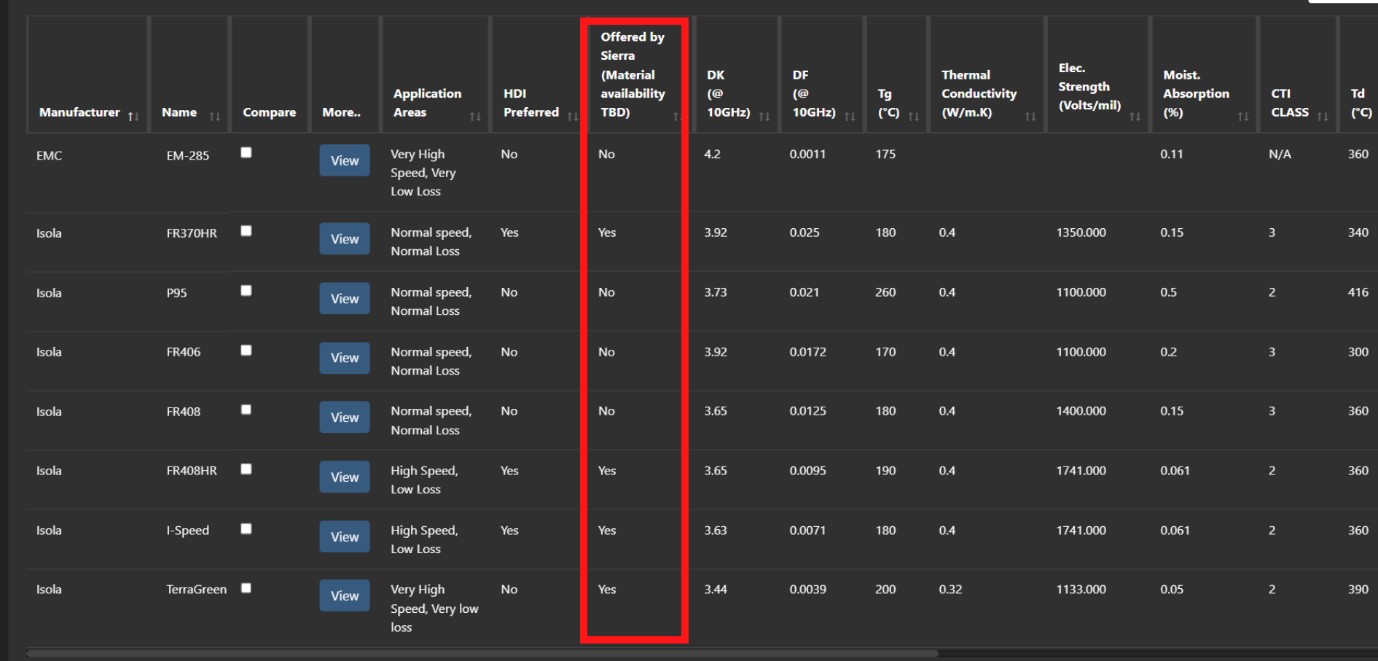
Does Sierra Circuits offer all the materials shown in the tool?
Every material displayed in the tool is not offered by Sierra Circuits. In the search results, there’s a column named Offered by Sierra to indicate the availability of the materials. Speak to our account manager (tel:+1 (800) 763-7503) to know about the availability of a specific substrate.
PCB Stackup Designer
What are the advantages of using the Stackup Designer?
The tool has an extensive library of manufacturable stack-ups. It automatically recommends the type of construction (foil or core) based on the material selected. You can also use the tool to design controlled impedance traces as it is linked to a 2D field silver-based impedance calculator.
Click here to learn more about the PCB Stackup Designer features.
How do I define the board thickness?
You can use the drop-down beside the target PCB thickness section to define your board thickness. You can choose from the following values:
- 031 inches
- 039 inches
- 049 inches
- 062 inches
- 076 inches
- 093 inches
What kind of customization is possible with the stack-up generated?
You can alter the following parameters after generating the stack-up:
- Material
- Finished thickness
- Layer count
- Technology (HDI/Standard)
- Layer combination
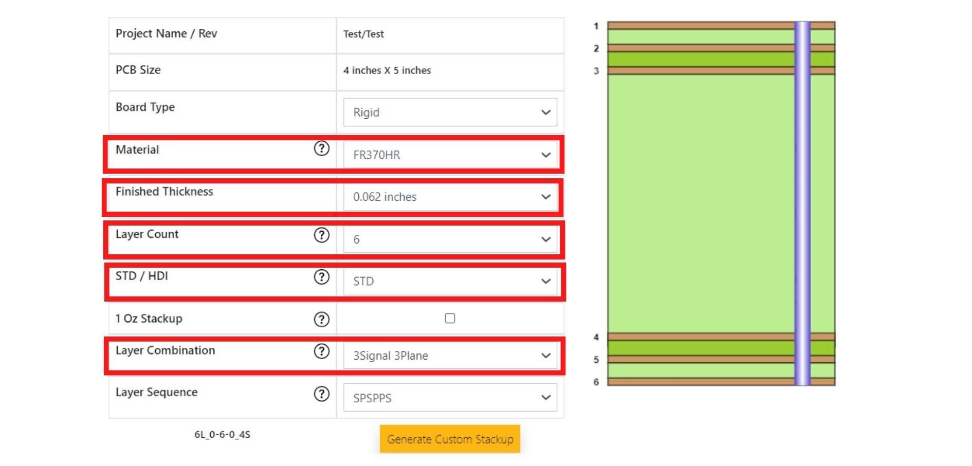
What is the difference between STD and HDI boards?
As the name suggests, HDI boards can accommodate high-density interconnection by incorporating blind and buried vias. The number in front of HDI indicates the number of sequential laminations. On the contrary, the standard boards only use through vias.
You can learn more about HDI PCB manufacturing from our Knowledge Base.
Impedance Calculator
Why should I use this Impedance Calculator?
This free tool is based on 2D numerical solutions of Maxwell’s equation and renders accurate results that are on par with industry standards.
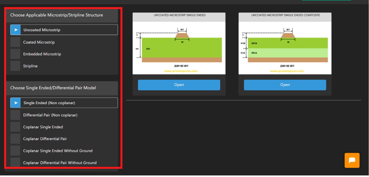
How many impedance geometries does this calculator support?
This Impedance Calculator supports 82 impedance models with multiple geometries such as coated, uncoated, and embedded microstrips and striplines. It also supports composite models which feature more than 1 type of dielectric.
What parameters can I calculate using this tool?
In addition to the characteristic impedance of a transmission line, you can also calculate line parameters such as trace width, propagation delay, capacitance, inductance, the effective dielectric constant of the structure, and in the case of differential pairs, coupling coefficient, and even & odd mode characteristic parameters. Recently, we have also integrated an in-built calculator to determine the signal loss for the given geometry.
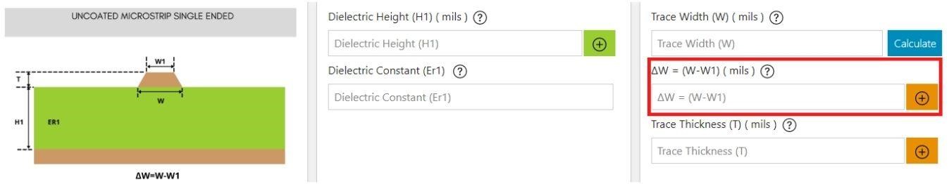
Does this tool take care of the etch-back effect (trapezoidal shape of the trace)?
Yes, the tool accounts for the trapezoidal shape of the trace. The delta w input field under the trace information section facilitates this.
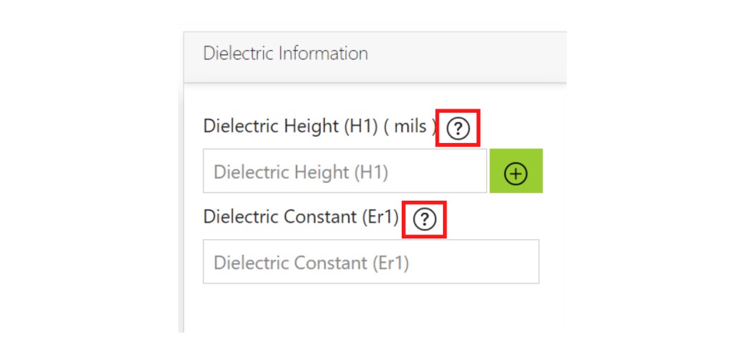
I don’t know what values to enter in many of the input sections, what should I do?
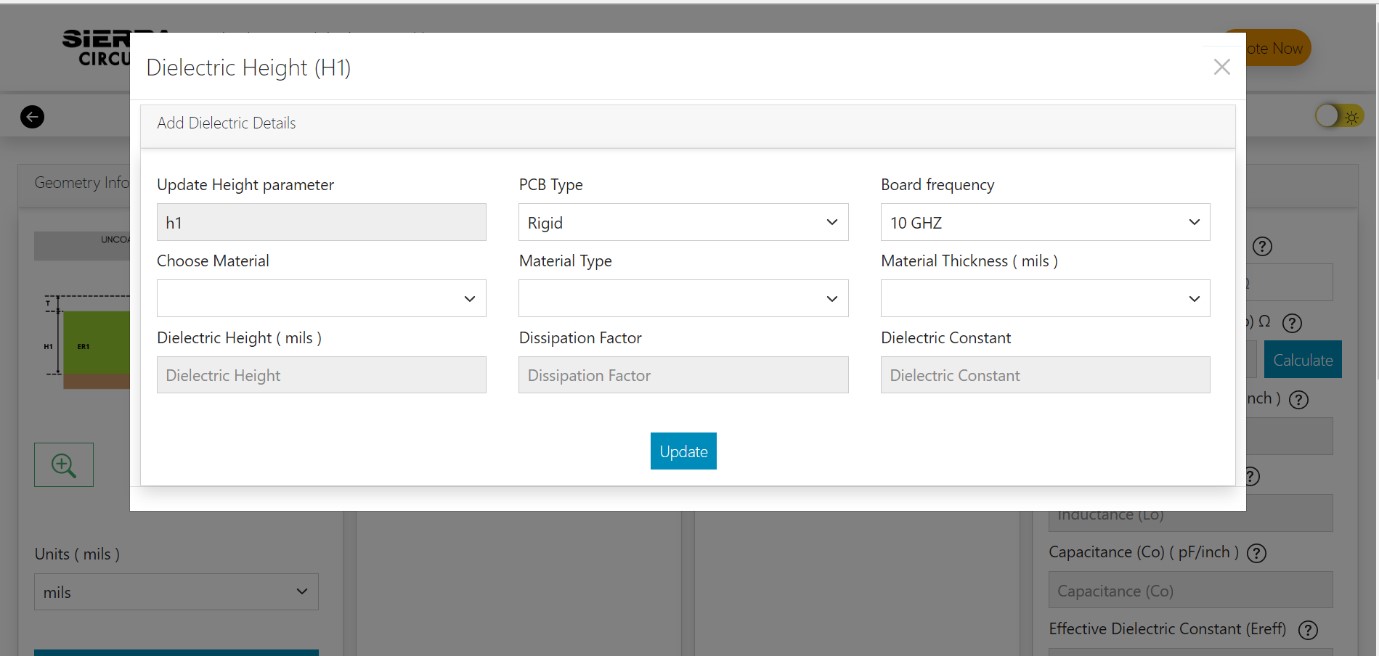
If you’re not sure about any of the input parameters, you can click on the respective help button. In addition to this, we have provided a dielectric material construction table to assist you with various dielectric information. The table includes the dielectric constant and dissipation factor of different materials at different frequencies, thicknesses, and resin content.
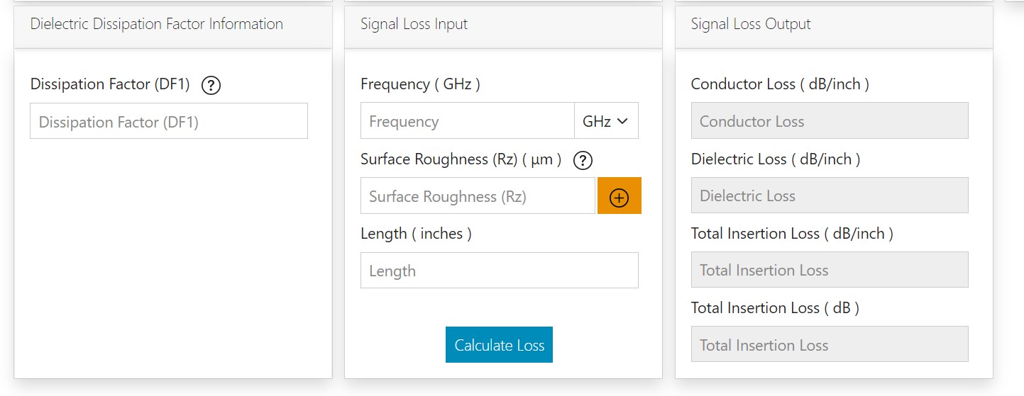
How do I access the signal loss calculator?
The signal loss calculator is integrated with the impedance calculator. You can calculate the signal loss by entering the input parameters (Df, frequency, surface roughness, and length of the trace) in the respective fields.
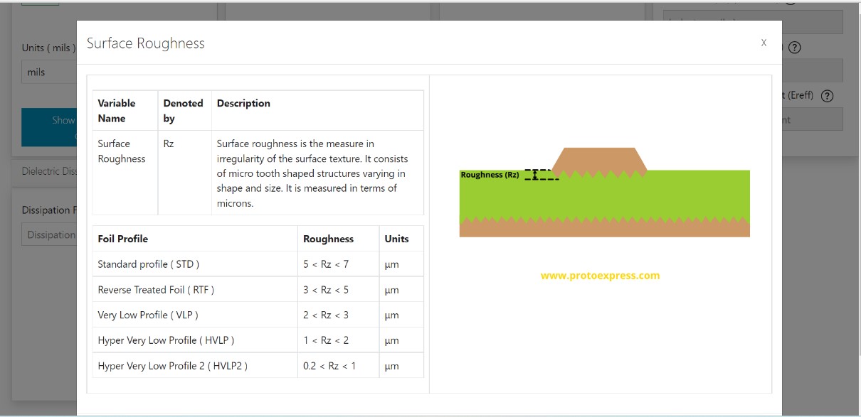
How does roughness affect the signal loss calculation and what values should I generally use?
Roughness becomes a significant contributor to signal loss at higher frequencies. If roughness is more, signal loss will be more at a given frequency. Copper foils come in different roughness grades. Refer to the table in the help option near the roughness input for more information.
Via Impedance Calculator
What is this tool based on?
The tool is based on numerical solutions of Maxwell’s equation.
What are the features of the tool?
The main features of this tool are:
- Allows you to choose between two via models: through-hole and laser.
- Each model supports four via structures (through-hole via and through-hole back drilled via).
- For the selected configuration, you can calculate capacitance, inductance, characteristic impedance, propagation delay, and effective dielectric constant.
Signal and Plane Layers Estimator
When should I use this tool?
You can use this tool to compute the optimum number of signal and plane layers when during the initial stage of your stack-up design.
What is the signal and plane layer estimator based on?
To calculate the required signal and plane layer, the tool uses multiple well-known estimation algorithms such as:
- Coor’s wiring length model
- Hannemann’s wiring demand model
- Geometric model (Moreseo)
- Rent’s rule
Trace Width, Current Capacity, and Temperature Rise Calculator
What is this tool based on?
Calculations are based on the IPC-2152. This standard is more precise compared to the previous IPC-2221 standard.
What are the unique features of this tool?
It is a 3-in-1 calculator that determines the temperature rise above ambient, trace width, and maximum trace current capacity. It also calculates resistance, voltage drop, and power loss of the internal and external traces.
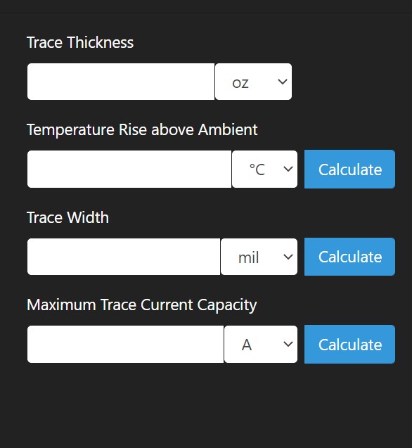
I am working on a high current board. How this tool is useful to me?
The tool can help you calculate the optimum trace width which can handle a high current without damage.
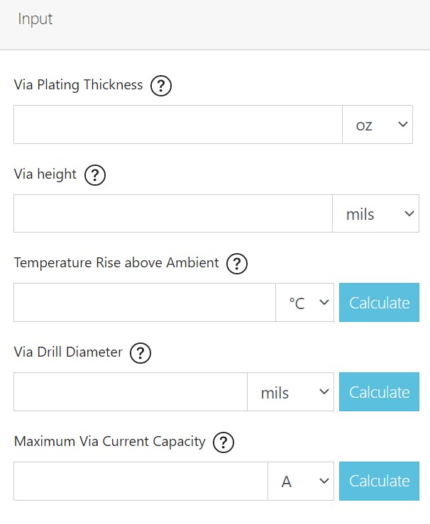
Via Current Capacity and Temperature Rise Calculator
What is this tool based on?
This tool is a derivative of the trace current capacity tool modified for vias. The trace current capacity tool is based on IPC-2152.
What are the unique features of this tool?
It is a 3-in-1 calculator for temperature rise above ambient, via drill diameter and maximum via current capacity. The tool also calculates the resistance, voltage drop, and power loss at the via.
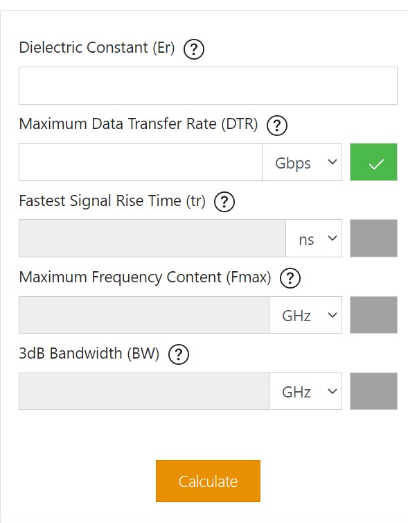
Maximum Via Stub Length Calculator
How does the via stub length calculator helps in board design?
In your design, if a via stub is greater than the acceptable length, it causes signal attenuation. This calculator helps you to determine the optimum length of the stub based on the frequency of the signal.
What are the inputs required for this tool?
You can calculate the maximum allowable stub length and its resonant frequency by entering the following parameters:
- Dielectric constant
- maximum data transfer rate
- fastest signal rise time
- maximum frequency content
- 3dB bandwidth
It also supports reverse calculation, which means that you can input desired via stub length and calculate any one of the above-said parameters.
RLC Resonant Frequency and Impedance Calculator
What is the objective of the tool?
The purpose of the tool is to calculate the resonant frequency of the RLC circuit along with capacitive, inductive, and resistive impedance at the input frequency.
Bandwidth, Rise Time, and Critical Length Calculator
How does the tool help in the design process?
The tool calculates the critical length of the conductor for the given signal rise time or the bandwidth, to reduce the signal reflection.
What are the important parameters required for the calculations?
The parameters required for calculation are:
- Dielectric constant of the material
- Rise time or bandwidth
- Maximum frequency content in the signal
Does the tool consider PCB trace coating/masks?
Yes, the tool considers coating details including the thickness and the dielectric constants. Choose coated microstrip geometry to calculate propagation delay, considering the mask specifics.
Transmission Line Reflection Calculator
What is the significance for this tool?
The calculator will display the voltage graph at the input and output of the Tx line. If there is an impedance mismatch, you can see ripples at both ends.
What are the ideal values for source, line, and load impedances?
Source impedance should be as low as possible. The load and line impedance should be equal to ensure zero reflection at the receiver end.
PCB Conductor Spacing and Voltage Calculator
What is this tool based on?
The tool is based on the IPC-2221B standard. It provides guidelines on the range of voltages and separations which may not be consistent. The calculator utilizes the IPC-2221B values and generates more consistent and realistic results.
What are the unique features of this tool?
The tool calculates the minimum spacing between two conductors with the potential difference between them as input. Conversely, if the spacing between two conductors is given then the maximum potential difference can be computed.
What all geometries are available in this tool?
You can choose from the following configurations:
- Conductors on internal layers
- External conductors uncoated
- External conductors uncoated (above 3050 meters)
- External conductors SM (solder mask) coated,
- External conductors with conformal coating
- Component leads uncoated
- Component leads with conformal coating
Can this tool calculate values in metric units?
Yes, the unit selection dropdown is available near each input. For the spacing, you can select units like inches, mils, mm, and cm.


