You may be surprised how cost effective small circuit boards are at scale.
Sierra Circuits’ engineers can help you efficiently produce your microelectronics boards in the United States. As a quick example, one way our engineers can help is by planning your stack-up early in the process—reducing your layer count by reducing your trace width.
Learn more about our services and capabilities for microelectronic PCBs.
Classification
How do I know if my board is classified as micro electronics?
The following specifications can be termed as micro electronics:
- 30 micron lines / spaces (1.25 Mils)
- Very thin film build up down to 1-mil thick
- Laser hole drilled as small as 2 mils
Where do I find these applications?
Mainly in flip chip packages, chip scale packages (CSP), and build-up substrates. The end applications are: smartphones, digital still cameras, and next generation compact packages.
Structure
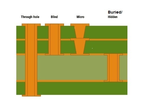
Can microelectronics have blind and buried structures?
Surface Finish
What is the surface finish of micro electronic PCBs?
The surface finish for micro boards is soft gold. Usually, we have a wire bonding process.
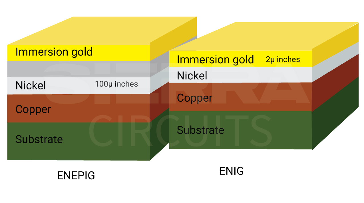
Is there a minimum thickness for the nickel or is it already covered under ENEPIG and ENIG?
Standard thicknesses are preferred. The thickness of nickel can be about a few hundred micro inches. Gold is about 2µ inches in ENIG, whereas soft gold can be about 30µ inches.


