Sierra Circuits helps you get to market faster with an engineering team who has been bringing to life the most reliable PCBs since 1986. Let us know how we can assist you and check our PCB design support FAQs.
High-current boards
What is the copper thickness range for high-current PCBs (>2 amps)?
1.4 mil to 2.8 mil is the copper thickness range for high-current PCBs.
What is the main factor that you should consider while selecting trace width and spacing?
You need to consider the copper thickness/weight when choosing the trace width and spacing. Bear in mind that line width is directly proportional to copper weight.
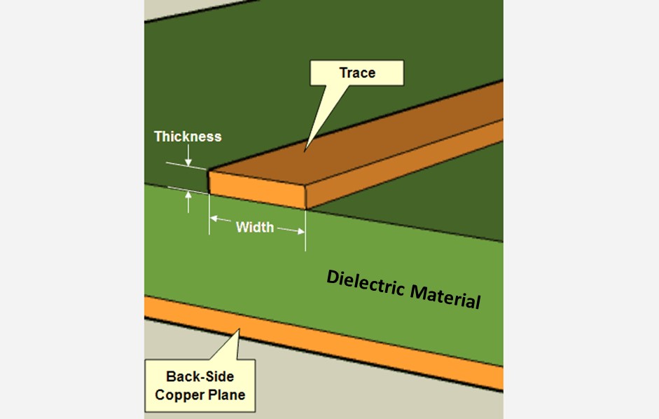
PCB trace width is proportional to copper thickness
The table below shows the optimum line width and spacing for a specific copper thickness.
| Start copper | Minimum capability in mil (outer layers) | Minimum capability in mil (inner layers) |
||
|---|---|---|---|---|
| Line width | Space | Line width | Space | |
| 5 micron | 2 | 2 | 2 | 2 |
| 9 micron or ¼ oz | 3 | 3 | 2.5 | 2.5 |
| ½ oz | 4 | 4 | 3 | 3 |
| 1 oz | 6 | 6 | 4 | 4 |
| 2 oz | 8 | 8 | 6 | 6 |
| 3 oz | 12 | 12 | 7 | 7 |
| 4 oz | 14 | 14 | 8 | 8 |
| 5 oz | 16 | 16 | 9 | 9 |
| 6 oz | 20 | 20 | 10 | 10 |
How do you calculate the physical dimensions of a trace that carries more than 2 amperes of current?
The conventional design approach for high current requirements is to widen the copper traces and increase their thickness to 2 oz. This would increase the space requirements and the number of layers on the board. For power and ground planes, employ wider traces of around 10 mil width. The maximum current carrying capacity for 2 oz copper with a temperature rise of 10°C is mentioned in this table below. Use the Trace Width and Current Capacity Calculator to compute the required trace width for your design.
| Maximum current capacity (amps) | Minimum trace width for external layers (mil) | Minimum trace width for internal layers (mil) |
|---|---|---|
| 2 | 19.95 | 20.03 |
| 4 | 66.59 | 66.86 |
| 6 | 134.78 | 135.34 |
| 8 | 222.28 | 223.21 |
| 10 | 327.68 | 329.05 |
How do you calculate creepage and clearance distances for high-voltage designs?
The creepage and clearance values are calculated by determining the working voltage under a specific operating voltage. As stated in various international standards, including IEC 950 and EN 60950, working voltage is the highest voltage across any particular insulation when the equipment is subjected to a rated voltage. While determining working voltages, you need to evaluate both peak and RMS voltages. Use the PCB Conductor Spacing and Voltage Calculator to compute optimum creepage for your high-voltage designs. IPC-2221 standard defines the benchmark for calculating the minimum spacing between two conductors to pass the required high-voltage.
![]()
Clearance and creepage distances between two PCB conductors
How many vias can be included in a high-current application?
For a high-current board, you need to optimize the number of vias to be incorporated depending on the drill diameter and current-capacity of the via. The greater the drill size, the higher the current carrying capacity of the via. If the board has space restrictions, increase the drill size to reduce the via count.
Use the Via Current Capacity and Temperature Rise Calculator to determine the exact number of vias for a given via diameter, plating thickness, height, current carrying capacity, and temperature rise over ambient.
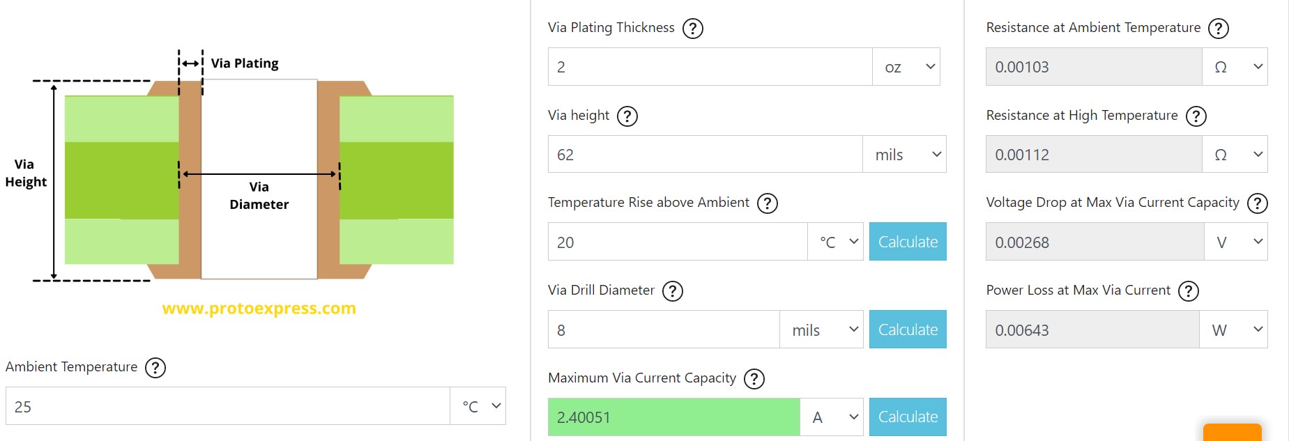
Via Current Capacity and Temperature Rise Calculator
Above example, we have calculated the maximum via current capacity to be 2.40051 amps, provided,
- Via Plating Thickness = 2 oz
- Via height = 62 mils
- Temperature Rise above Ambient = 20℃
- Via Drill Diameter = 8 mils
- Ambient Temperature = 25℃
Therefore, if we are designing a board with 10 amps of operating current, we need to employ approximately 5 vias.
I'm working on a high-current board with a finished copper of 3–4 oz. Is this also a high-speed one?
High-speed and high-current are two separate domains. When you are talking about high current, it is related to the power of the conductor. On the other hand, for a high-speed design, you need to focus on impedance, propagation delay, and signal loss analysis.
Schematics
What’s the first thing to consider while naming and numbering the pins in a schematic design?
While creating a schematic library, you need to ensure that the pin names and numbers match the ones in the OEM’s datasheet.
Transmission lines
What are the differences between single-ended and differential pairs?
Some of the significant differences between single-ended and differential pairs are enlisted in this table.
| Single-ended (SE) signaling | Differential pair signaling |
|---|---|
| Carries signal that is referenced to the ground plane. | Two traces are used to carry the signals. Signals carried by differential pairs complement each other. |
| Used in computer and peripheral communications such as VGA, PCI, keyboards, motherboards, SCSI hard drives, RS-232, DDR, and inter-integrated circuit (I2C). | Used in HDMI, USB, Ethernet, DDR, RS-422, RS-485, SDI, and twisted pair cables and low amplitude signals. |
| Easy routing process and requires less area to route. | Consumes more space. Routing is more complicated than SE traces. |
| Common-mode noise is a critical issue here that typically appears on the ground plane. | Common-mode noise is generated with equal amplitude and opposite polarity. Hence the noise on both traces gets canceled out. This minimizes the noise, EMI, and crosstalk. |
Where are the coplanar wave guides generally implemented?
A coplanar waveguide structure has the signal trace and the return path conductor on the same PCB layer. Low-loss coplanar waveguides are quite popular in RF boards where the signal is routed to an amplifier, antenna, or mixer.
Coplanar structure in Altium Designer tool
Stack-ups
How do you calculate the finished thickness for external layers?
The finished PCB thickness for the external layer takes into account the copper foil thickness and the plating thickness as well. Remember to add the outer layer plating thickness when you’re arriving at the finished thickness to avoid discrepancies.
The foil thickness for the above stack-up is 0.25 oz, or 0.34 mil. The finished thickness for the external layers can be computed as (foil thickness + plating thickness) = ( 0.35 + 1.15) or 1.49 mil.
DFM
What should be the minimum solder mask thickness?
The minimum thickness for a solder mask is around 4 mils. At Sierra Circuits, we also ensure that the ratio of the pad to the solder mask openings is 1:1 to avoid exposure of the ground plane next to the pad.
What should be the minimum silkscreen height?
We recommend a minimum of 25 mil height for legible silkscreen legends.
PCB testing: Flying probe testing
What’s the maximum number of pins and vias your FPT machine can handle?
We use Seica’s flying probe testing machine that can handle over 60,000 pins and vias.
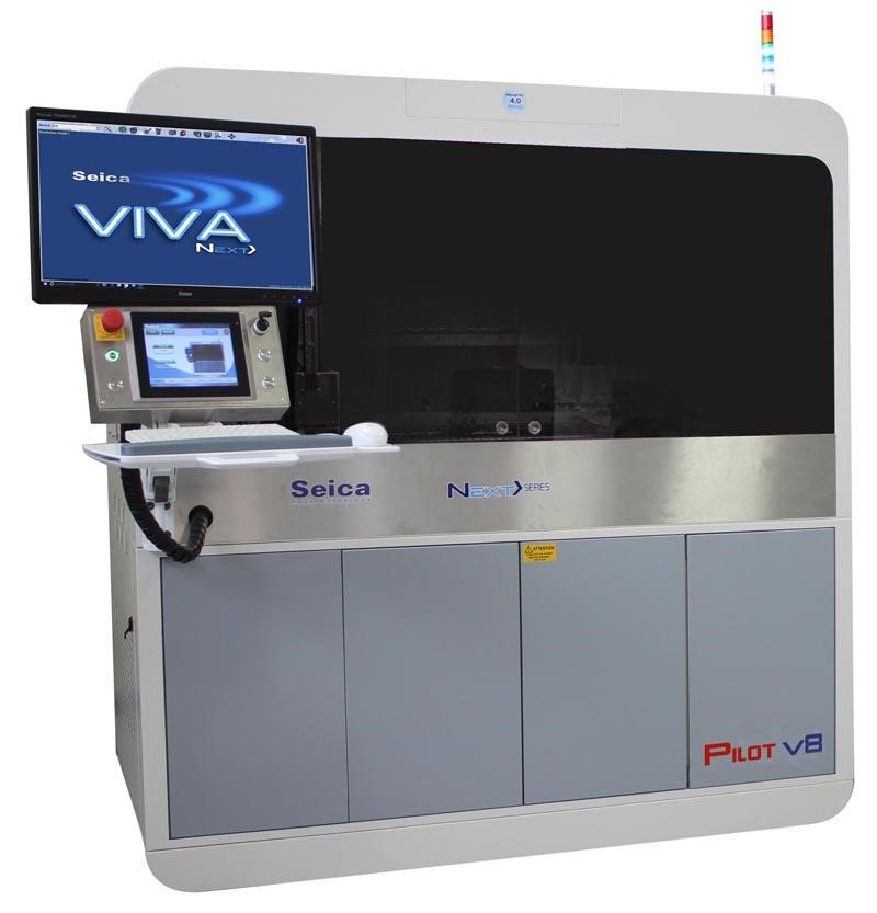
Seica Spa Pilot V8 FPT machine – Image credit: Seica
What is the workmanship standard used for flying probe tests?
The workmanship standard for flying probe testing depends on the following:
- Misplacement of components
- Mounting a defective component
- Excessive or insufficient solder mask
- Improper pad sizes, which leads to tombstoning
- Appropriate gap between components and between components and board edges
Can FPT detect voltage drops on the circuit board?
No, it doesn’t. A voltage drop can only be detected by a functional test. However, if the board is powered up, you can measure the voltage drop by using a voltmeter to check from point to point against the ground.
Can you probe fine pitch components using FPT?
Yes, fine pitch components can be probed if it sits on the pad and leaves about 6 mm on each side.
Is testing necessary for prototypes in PCB manufacturing?
Testing, specifically the Flying Probe Test, is recommended for small batch prototypes as it confirms the quality of workmanship on the board. While it does increase costs, the increase is not that significant.
PCB assembly: BOM
How to ensure a clean BOM?
For creating a clean bill of materials, you need to specify component details such as name, value, description, manufacturer details, MPN, and mounting technology. These are represented by simple text strings called line items.
Use the BOM Checker tool to create a clean BOM for PCB assembly. This tool points out the errors associated with the uploaded material list. It also gives you an idea about the availability of the parts and their life cycles from a set of vendors.
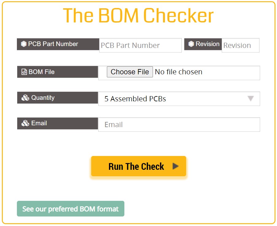
Sierra Circuits’ BOM Checker tool
PCB assembly: Layout and design
What are the preferred component clearance values that should be incorporated in my layout?
If the required component clearance is not stated in the design, the default component clearance would be 10 mils. Here are the clearance values for different components:
- Clearance for BGA devices: 20 mils
- Parts smaller than 0603 packages: 6 mils
- Connectors, crystals, and canned capacitors: 20 mils
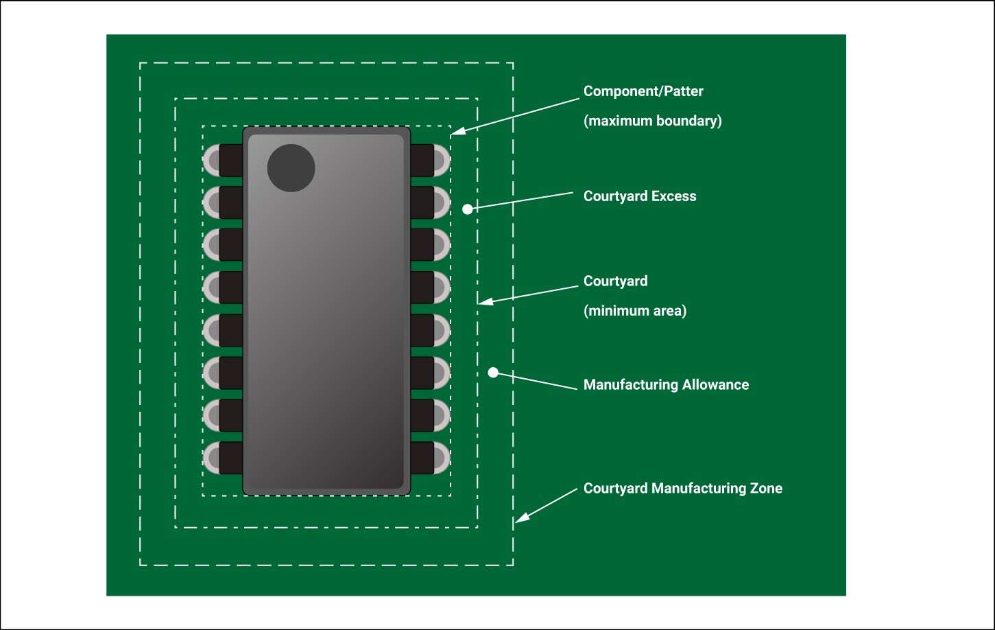
Component boundary
What is the optimum spacing for the solder mask to be offset from the pads in order to prevent soldering errors?
We generally adhere to the 1:1 rule (the solder mask and pad are of the same size). If this is not possible, we can have 2 mils of offset to solder mask from the pads on each side.
PCB assembly: Certifications and standards
What are the PCBA visual inspection and rework certifications that apply for IPC class 2 PCBAs?
IPC-A-610 defines the benchmarks for visual inspection and rework of class 2 circuit boards. At Sierra Circuits, we also provide a Certificate of Conformance for Class 2 designs when we ship the assembled board after verification by the certified inspectors.
High-speed boards: Dielectric materials
Why are low Dk materials preferred in high-speed applications?
Low Dk materials are preferred in high-speed applications for the following reasons:
- Offers low-loss tangent at high frequencies
- Reduces crosstalk between closely spaced traces and vias
- Limits the need for capacitive coupling in the circuit
- Lowers the adverse effects of mismatched trace lengths in parallel nets
To know more about high-speed material characteristics, see high speed PCB materials: Rogers 4350B and Panasonic Megtron 6.
High-density interconnects: HDI fabrication
When should I prefer foil construction over core construction?
When you have microvia and sequential lamination requirements, foil constriction would be the appropriate choice to prevent moisture flow between the adjacent layers.
Is there any plating requirement for the lower staggered vias?
For the staggered structure, via filling is not required for the lower vias. But in the case of stacked, conductive via filling is performed.
How much can the maximum data rate and the number of staggered vias be for high-speed differential signaling?
The maximum data rate for high-speed differential signaling depends on various factors, such as layer sizes, dielectric material used, and aspect ratios. In general, serial data rates can be increased to several GHz. The via count and data rate are inversely proportional to each other. More vias equal less bandwidth, while fewer vias equal more bandwidth.
Flex and rigid-flex: Stack-up for flex PCBs
Can you build a 3-layer flex board with controlled impedance?
Yes, we are capable of fabricating a 3-layer flex board with 50 Ω controlled impedance with 5% tolerance.


