Sierra Circuits is the nation’s top HDI PCB manufacturer — with expert engineering and rigorous testing to deliver full turnkey HDI PCB assemblies guaranteed to work.
Choosing HDI
Why should I turn to HDI?
At some level of circuit complexity, turning to an architecture with blind and buried vias will result in better yield and lower cost than would a through-hole design.
HDI Cost Considerations
How does HDI keep my cost down?
One of the problems designers face is keeping cost down. Our goal is to provide some insight to help you with your decision-making process. When making PCB design decisions for HDI, one of the primary concerns is in regards to manufacturability and cost. Just like standard PCB designs, HDI boards have four main concerns:
- Materials
- Layers and laminations
- Vias in HDI classes
- Optimal trace and space
What is the most expensive stack-up class?
The more sequential laminations, the higher the cost. The most expensive stack-up class is three sequential laminations. This includes microvias stacked on top of each other, which is necessary when you are breaking out of a tight pitch BGA, like .3 mm. Second in the stack-up class in terms of cost are using a non-conductive hole through process.
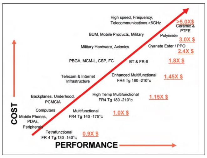
Selecting HDI Materials
How do I select materials for HDI?
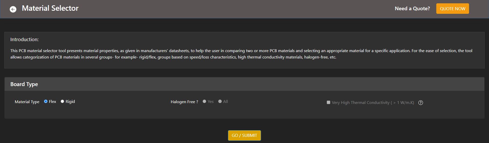
Materials play a large role in terms of manufacturability and direct cost of your circuit board. Here is a tip: The goal is always to select the right material for manufacturability that, at the same time, meets your temperature, and your electrical requirements. When it comes to materials, make sure that your high-speed material is also suitable for your HDI design. They are many other factors that come into play when selecting the proper materials for your design. Use our free Material Selector to find out which materials will suit your application the best.
What should I keep in mind when choosing layers and laminations?
When thinking about layers and laminations, keep in mind the following questions: Have you planned your layer sequencing for reduced EMI? Have you decided your routing density? What is the total number of sequential laminations? And have you minimized your laminations?
What should I keep in mind when choosing my via structure?
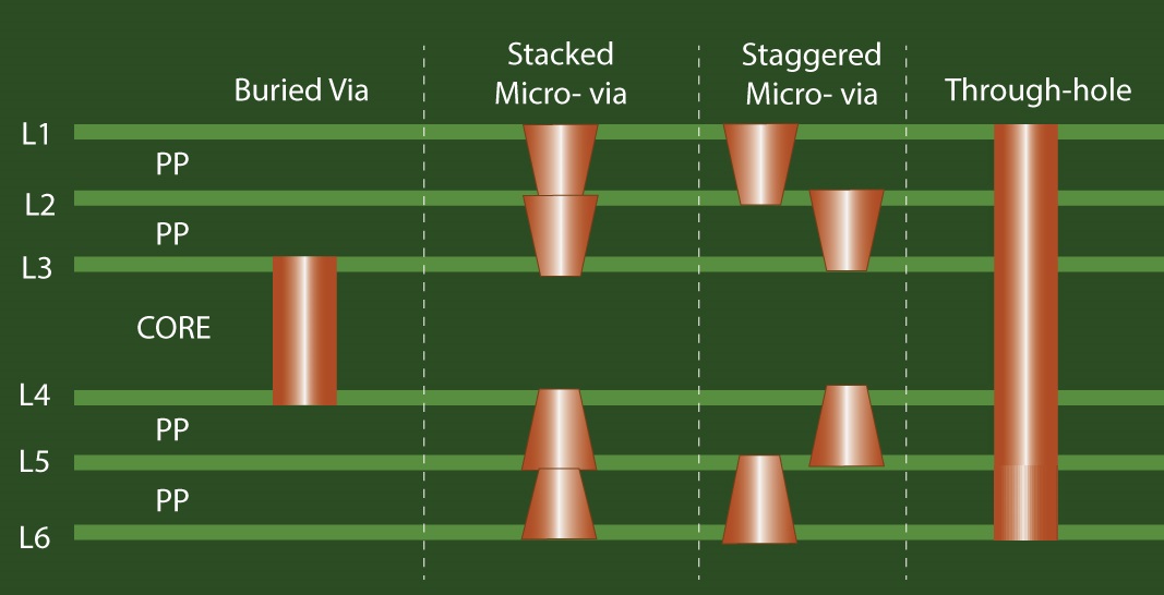
Manufacturability primarily has to do with via structure. Answer the following questions before you start working on your next project: Are you meeting the design guidelines for microvia aspect ratio? Are you stacking or staggering your microvias?
How does FR4 or other dielectric materials withstand capabilities that degrade over time?
There is no scope of short-term failure or a long-term failure. As you get through the multiple lamination cycles, you may see a degradation of the first lam cycle, and it may fail during thermal stressing and final inspection. But again, a higher Tg material is a good choice. Many of the FR4 materials like 370 HR, have higher Tg than a 406 material. It can withstand multiple lamination cycles. A polyamide material, which has higher Tg can withstand more lamination cycles also.
Does it matter what material you use if you're stacking the vias? Does that make a difference?
Not really. There is no correlation between the material type and whether the vias are stacked or offset.
HDI Fabrication
What should I keep in mind when choosing the trace and space?
And lastly, trace and space. Have you considered reducing your trace width to increase density and ultimately reduce your layer count? Here is a brief plug on Sierra Circuits: If you are considering reducing your trace width to increase density and reduce your layer count, 2-mil trace and space may be exactly what you are looking for. Our yields are 90% for this density.
When it comes to the manufacturability and the cost of an HDI board, it is very important to remember that none of these considerations can be dealt with in isolation. For example, reducing your trace and space will always ultimately reduce your layer count. Or, how can you plan your via and pad sizes which impact the space you have to route your traces?
How do I choose between mechanical or laser drill?
Drilling is the huge cost driver. A lot of factors can impact your decision. To name a few, there is the cost of the drill bit, the time it takes to drill mechanical holes, and the quality of the drill. A 6-mil drill is much more expensive when compared to a 10-mil drill. What can make this process even more complex is the use of hybrid materials. For hybrid materials, each material requires a different drill cycle and plasma cycle. Bottom line, if you have the opportunity to reduce or eliminate mechanically-drilled vias and use laser-drilled microvias instead, you could save a tremendous direct cost for yield.
When do I use mechanical via vs laser via?
Mechanical drilling:
-
- Mechanical drilling provides vias with higher aspect ratios.
- They have a minimum drill diameter of 5.9 mil.
- These are less expensive and wear out quickly.
Laser drilling:
-
- Laser vias provide vias with a smaller aspect ratio.
- They have smaller drill diameter in the range from 0.008″ (0.20mm) to 0.001″ (0.025mm).
- They can fit into tight land areas within tight pitch SMT or BGA footprints.
- Generally, the aspect ratio of laser vias is 0.75:1. Laser drilling is required for vias with a smaller diameter. When the BGA pads are equal to or less than 0.5mm, it requires laser-drilled microvias as the pad diameter is too small.
- Laser vias are used to form blind and buried vias in sequential lamination. They are often used with fine pitch BGAs.
If you need to select laser vias or mechanical vias, then you need to consider the size and substrate material. Another factor is the fixed and variable costs that need to be analyzed. Mechanical drilling has lower fixed costs whereas laser drilling has lower variable costs.
What is the range of laser drilling?
We can do minimum of 4 mils and maximum of 8 mils holes using laser drilling.
How do I choose between conductive and non-conductive hole fill?
Do you have vias underneath a surface-mount component that is required to be filled and capped or plated over? It is costly because it requires two plating steps and two drill steps. We drill holes that will be filled separately from the regular through-holes on the board and any extra steps mean extra cost. In this case, we are going back to the process twice, which costs in terms of time and dollars, drilling and plating.
How do you design HDI for thermal-mechanical stresses with multiple layers?
It depends on the number of lamination cycles the prepreg goes through, and there is a maximum limit. The lamination parameters should be considered during every cycle. The number of lamination cycles puts additional stress on that prepreg. If the material is not properly cured, the via structures will be affected during the drill cycle. We’ve been successful in designing the boards up to 4 or 5 lamination cycles. We would suggest using a higher Tg material when the number of cycles is greater than 3 or 4. The thicker the board, the more expansion of the material. This also exerts more stress on the interconnects and the vias.
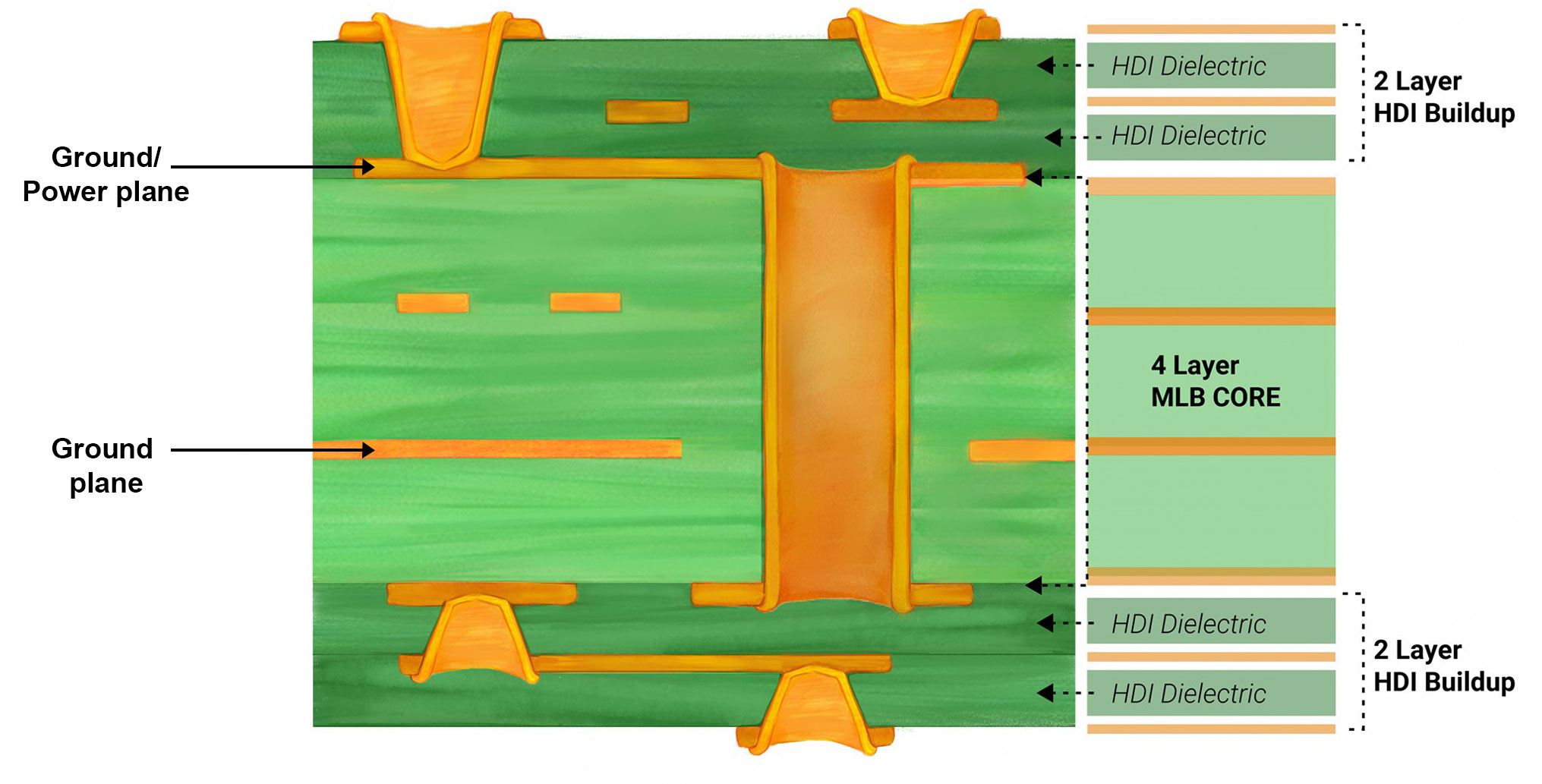
Some designs use PCBs as thermal paths for power parts. This may require multiple ground planes. What is the maximum number of planes (power and ground) for HDI designs?
IPC-2221 and IPC-2222 will help you with the thermal ties to planes. Typically, the number of laminations in HDI is limited to maximum 4 with inner lamination being a core structure. In the core, you can have multiple power and ground planes. However, in the laminations, this could be a maximum of 2 on either side. But typically, 1 ground and power plane is recommended.
What is the minimum trace width for harsh environments, like J-STD-001ES?
Due to small features (trace and space) of HDI designs, we use quarter-ounce foils, sometimes even less than that, to hold the fine traces. We typically use a minimum of 3 mils trace width. But if the design requires, we can go further down. However, it is not recommended to go below 3 mils.
What are the failure modes for stacked vias? Why should we avoid stacked vias?
Generally, a lot of designs require stacked vias because of their density. When we conduct interconnect stress testing (IST), it is observed that stacked vias fail sooner than offset vias. This might be due to the mechanical characteristics. Also, the connection between copper-filled microvia and the contact pad fails on the stacked vias, but it remains the same with offset vias.
What is the required staggered via spacing?
If you are staggering a microvia or a laser via, you need a minimum spacing of about 2 mils between the two vias. The spacing between a laser and a through-hole via should be 3 to 5 mils.
For ultra high speed (30 GHz), staggered vias and the non-functional target lands can be a problem. Those speeds don't like irregularities. Any suggestions for mitigation? How deep can you stack the microvias?
We remove non-functional pads unless prohibited. For a stacked via, you must have a landing pad. In that case, we would add a pad. We build a lot of stacked vias that go all the way through a board, perhaps even up to 8 or 10 layers deep. It’s about the difference in reliability when you stress them through an IST or multiple thermal excursions. In many cases, those stacked vias will not fail. But when we stress them on an IST, they fail sooner than those designs without stacked vias.
Could you explain about class 3 pad and via sizes in detail?
The size of a pad required to meet a mid-annular ring is different for a double-sided board or 4-layer board than it is for a 16-layer board. But for class 3, we need 6, 7, and 8 mils of an annular ring before drilling. It depends on the layer count and the number of lamination cycles. Generally, finished hole size and a pad size are given. We have to increase the drill size for plating. So, that cuts into that amount of annular ring over the drill size. If you don’t have a strict requirement for tolerance on a via, it’s always best to take the finished size with a tolerance of ± 2 mils the via size. Normally, the drill size is 3 to 4 mils larger than your finished size.
What is the preferred approach for blind via and mechanically drilled through-hole via: SMT or BGA?
We can make both in case of blind via using laser drilling copper filled hole. For mechanically drilled holes non-conductive filling is used.
Microvia Considerations
What are the critical dimensions of a laser-drilled microvia?
The critical dimensions are the pad size, the laser drill size, and the press-out thickness of the dielectric. You must define your laser drill size in proportion to the finished press-out thickness in order to properly plate the via. Laser drill dimensions can get very small. But remember, they are only going from one layer to the next. Many fabricators can laser a 2-mil hole but plating the 2-mil hole becomes problematic because of the aspect ratio of the thickness due to the drill diameter of the hole.
What is a preferable design approach for microvia?
Staggered is better than stack-up approach, as in this case, we can avoid some processes like filling all sequential lamination and laser-drilled holes. We prefer staggered over stack-up to design microvias with sequential lamination.
What is the difference between microvia and mechanically drilled via?
Laser drilling depends on aspect ratio and the finished hole diameter. Eg. If the finished hole diameter is 4 mils and the distance between the two layer is 4 mils or less than that, we can do laser drilling then. Otherwise we have to go for mechanical drilling. Laser drilling depends on aspect ratio and finished hole diameter.
Which IPC document defines the drill size for microvias?
IPC-6012 defines the drill size for microvias.
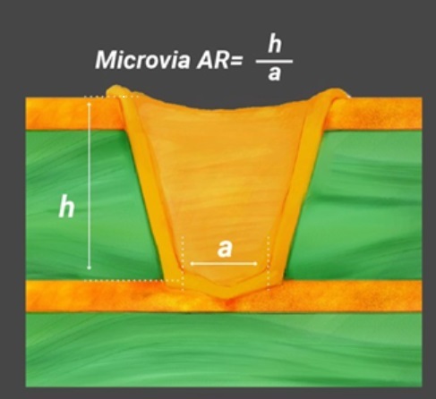
What is the optimal aspect ratio?
You want to stay 0.75:1 to ensure a good plating. The shape of the microvia is important to allow for the plating solution to flow properly and plate or fill the microvia. If you have to do build-up, or in another word you need a buried via, then you would need to choose between staggered or stacked vias.
What is the difference between staggered and stacked microvias?
Staggered vias essentially mean fewer process steps. We do not have to fill the laser-drilled vias with copper because the second laser drill does not land on the first laser drill. Filling or plating a microvia shut usually happens in a special plating tank designed with chemistry that plates the laser-drilled microvia from the bottom of the via to the top of the via, until it fills the hole completely. Plating a laser-drilled microvia shut adds time and cost to the process. You only need it when you are stacking on an inner layer. Or if you have a via-in-pad on the outer layer. If the second laser-drilled via is staggered or offset, there is no need to copper plate shut. If you are staggering your laser-drilled microvias, it is important to know what spacing your manufacturer requires between the laser drills.
How close to 50 ohms is a microvia?
The closeness of impedance depends upon the design of the microvia. This depends on the microvia width, anti-pad, and plating. The tolerance could be within ±10%.
How can you get microvias to match 50 ohms?
The impedance of a microvia is a function of diameter and copper weight (to a small degree). The most important factor is the spacing between the signal via and the return via. The transmission line consists of a trace and a return path. When you design a transmission line of a 50-ohm impedance, You need to design the pair to be 50 ohms instead of designing the signal trace to be 50 ohms. If you’re going on either side of a ground plane, a return via is not required. But if you’re going deeper into the board, the return via is needed. So, the key to control impedance is the size of the via relative to either the ground plane, or its spacing to the return via. There are field solvers (polar) which can measure the via impedance.
Can you have microvias with ceramic materials?
We do not process pure ceramic. But we do microvias using ceramic fill like Rogers 4000 series, 3000 series, 6000 series with laser vias.
Laser Drilling
What is the laser drill accuracy?
It is very safe to assume it is +/- 1 mil accuracy. Usually, in a staggered microvia formation, the diameters of both operate and lower microvias are the same. The key parameter that decides whether the staggering is possible or not, without the lower microvia needing to be filled, is the dimension E, the vertical separation between the central access of the two microvias. For staggering to be viable, the value of E must be greater than the microvia diameter.


