We are more than your PCB manufacturer. We help you flex your design potential. Get low-to-high volume flex and rigid-flex PCBs manufactured with industry leading quick turnaround times.
Advantages of Flex PCBs
What are the advantages of using flex versus cables?
Flex provides several advantages to cables. Flex’s higher upfront cost will dramatically reduce cost in the long run. Cables can take several weeks to go through production, while flex PCBs can be completed in several days. In short, using flex eliminates or completely decreases cable cost, reduces assembly time, and produces a lighter end-product.
Could you show some examples of applications that use flex?
Small form factor products which have constrained space and cannot accommodate connectors are ideals for flex boards. These applications include mobile phones, watches, laptops and their screens.
Flex PCB Cost Considerations
What is the most cost-effective type of via for HDI rigid-flex designs, stacked microvia or blind/buried vias?
The real cost driver is the number of laminations. Vias should never be in an area that is dynamic. You don’t have to use stiffeners, but we do not suggest it in the flex area. Make sure vias stay out of the bending area as well.
What is a suitable approach for laminating a 6-layer rigid flex board?
We can do sequential lamination, from 1 to 2, 2 to 3, 3 to 4, 5 to 4, and from 6 to 5.
We will use sequential lamination for tightly spaced HDI boards.
What is the cost delta between class 2 and class 3 products?
Class 2 products follow a very basic manufacturing process. However, the class 3 manufacturing process has various checkpoints. Each and every class 3 board should undergo cross-sectional analysis. The cost of a class 3 circuit board could be 25% more than the class 2 build. The cost also depends on the manufacturers.
Materials
What are the best flex prepreg materials?
No-flow prepreg is the preferred bonding material for joining flex and rigid materials. This is most commonly found in standard FR-4 or Polyimide.
What are the alternative prepreg materials for joining flex and rigid materials?
No flow prepreg is the preferred bonding material. Available in either standard FR-4 or Polyimide.
What are the special flex materials used in patient contact medical devices?
We use Dupont material to build circuit boards for medtech applications that come in contact with patients.
Can you talk more about choices of flex substrates? How does the thickness affect flexibility of the flex circuits?
The flexing ability of a flex board mainly depends on the thickness of the copper layer and the substrate. Flexibility decreases as the thickness of the circuit increases. Cross hatched planes can be used to improve flexibility. This also is an ideal option for controlled impedance designs.
How to prevent cracking of vias because of thermal cycling?
The cracking of vias during thermal cycling can occur due to high CTE contrast at Z direction between resin and copper. This can be mitigated by choosing matierals with similar CTE values.
What are the preferred hole and pad sizes for flexible PCBs?
Some flex materials, like Kapton, do not drill as well as regular materials. 10 mils and above is preferred for minimum size, only in the flex part. Rigid-flex specs are similar to rigid board specs. Pad size, plating process for flex is barrel-only (hole wall).
How to avoid blistering?
Flex material is hydroscopic (it absorbs moisture). Blistering comes from moisture trying to get out, and can cause thermal defects, like substrate blisters and barrel cracking during soldering. It also reduces dielectric breakdown voltage and expands the board. Pre-bake can stop blistering and eliminate moisture absorption.
Stack Up for Flex PCBs
What does a real stack-up look like? (Not four signal layers, plane layers needed)
The plane layers for the flex are the same as the would be for the rigid board. This board would be turned into a 6-layer board, as follows:
Do you recommend thicker prepreg layers to join with the coverlays?
The total prepreg thickness must be greater than the coverlay thickness by at least 2 – 3 mils. If you have 2 mils of coverlay, you would need 3 – 4 mils of prepreg.
How many layers can your flex region have? Can you have hashed ground planes on either side of the signal layers for noise purposes?
The number of layers depends on the design requirements. 12 layers of flex is not unheard of; however, the higher the number of flex layers, the more difficult it is for the PCB to flex. Yes, you can have hashed ground planes on either side of the signal layers.
Designing & Manufacturing Flex PCBs
Are there any design rules for placing parts on the flex circuit?
Place parts where the flex has a stiffener or has been rigidized.
Are there recommended dimensions for the hatch pattern?
8 mils by 8 mils
Where are dimension tolerances specified?
Rigid-flex can generally hold the same tolerance as rigid PCBs. If you are talking about mechanical dimensions, +/- 5 mils is an acceptable tolerance.
Is it possible to create a flex section with exposed adhesive so the section can be attached to an interior surface of the enclosure?
Yes, pressure-sensitive adhesive (PSA) can be applied to flex.
How do you add a fully rigid panel around the outside of the rigid-flex design to aid in automated processing?
The rigid part of the board is also part of the array.
When manufacturing rigid-flex, how is the rigid part removed around the flex board?
The bonding material (prepreg) is removed from the flex region, and then the rigid part is milled as part of the final route operation.
Can flex handle high voltage (2-3 kV)?
Yes, 1 mil Kapton material can handle 5kV.
What options do blind and buried in flex allow?
This depends on how critical your design is. Flex can handle buried vias. If there is a combination of buried and blind vias, it is recommended to stagger the vias as flex boards bend during their operation.
What is the operating temperature range of flex PCBs?
Flex circuit boards can generally handle temperatures upto 350°F (177°C). If these circuits are exposed to higher temperature for a long time, the substrates start melting. The choice of materials is critical for high-temperature flex PCBs, as they must withstand thermal stress and material degradation
Do copper and core thicknesses impact the minimum bend radius?
Yes, copper and core thicknesses affect minimum bend radius.
How do you control drilling depth to drill blind vias?
We have advanced machines in our facility to perform the drilling process. These machines can drill vias with controlled depth as low as 1.5 mils.
What should be the minimum trace spacing in FPC?
The minimum trace spacing required in FPC with 1 ounce copper is 4 mils.
Can we implement via-in-pads in flex boards?
Having via-in-pads in a flex board completely depends on your design. For a two-sided board, the via can be drilled from the bottom side without disrupting the pad on the top layer. For a multilayer board, a dog bone architecture can be implemented. Here, the trace will be routed away from the pad towards the via. Via-in-pad is not recommended in the multilayer flex boards as it is required to planarize the copper surface after via filling. If planarization is performed on the flex materials, there is a risk of damaging the substrate.
Can you have overlapping flex layers that are not laminated/glued together?
Yes, this type of construction is called loose-leaf construction or air gap construction method. In this method, the flex layers are kept as several independent sets of no more than three layers per set. IPC 2223 document defines the standard for this type of structure. Air gap construction can overcome the mechanical and electrical reliability issues in higher layer count rigid-flex designs.
Can you produce an adhesive backed flex circuit that would adhere to a flexible mechanical component?
If you would like to bond a finished flex circuit to an external frame/structure, pressure sensitive adhesive (PSA) can be used. Please, email us for more information.
How do the typical lead-times compare between rigid only, flex only, and rigid-flex?
Rigid and 2-layer flex boards can be fabricated in 24 hours. The typical turnaround time for rigid-flex is generally 5 to 10 days depending on the requirements.
How does a silkscreen affect the flex properties of the board?
Silkscreen doesn’t affect the flex properties of the board.
How do you address potential thermal problems in a hybrid PCA design (due to different CTEs)?
We only use no flow prepregs to build hybrid (rigid-flex) circuit boards. The bonding of these materials comes with various constraints. One simple solution to address this issue is to select the materials with similar CTE values.
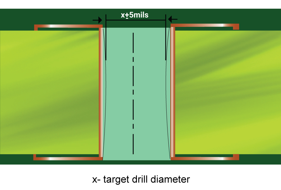
In a rigid-flex board, what is the minimum pad and drill size in the rigid section and in the flex section?
The minimum pad size for the rigid region in a rigid-flex board is D + .014″. And the minimum pad size for the flex section is D + .014″. Where D is the finished hole size. The value of D should be a minimum of 6 mils for mechanical drills.
What is the minimum laser drill for blind or buried vias in the rigid section of a rigid-flex PCB?
In the rigid section, the minimum laser drill allowed is 5 mils. Pad size is D + 4 mils. Where D is the finished hole size. Please note that laser drills are not allowed in the flex area.
Stiffeners
What is the purpose of stiffeners?
First, it is important for you to understand that the PCB stiffener is not an integrated part of the electrical circuit board design. It exists just to offer mechanical support. We call a stiffener for when you need it. Here are some enlisted reasons to call for stiffeners:
- Strengthen any specific area of the board.
- Maintain proper thickness in the flex circuit.
- Support PCB components and connectors.
- Constrain the flexible parts to areas where they should be.
- Facilitate better handling of a thin flimsy circuit board.
- Keep certain areas of flexible circuits flat and stable.
- Ensure compliance with ZIF connector specifications.
- Add flexibility to bend the radius of the circuit at the intersection of rigid and flex parts. This will avoid the stress on the flex part during multiple bending operations.
Basically, you use a stiffener when you require a rigid area in your flex circuit, maybe to protect components or connectors attached there. This will not let the circuit bend and protect the integrity of the part’s solder joint.
What is the typical stiffener thickness that should be considered while designing a flex board?
The standard stiffener thickness varies from 0.002′′ to 0.059′′. The FR-4 stiffeners can be 0.008″ to 0.059″ thick while the Kapton stiffener thickness ranges from 0.002″ to 0.010″. The more support the PCB stiffener provides, the thicker it is. Each design requires a distinct thickness.
Flex Assembly
What is the difference between assembling flex and rigid boards?
Flex is more difficult to assemble than rigid boards, because it is not as sturdy to assemble. We often create backing or fixtures to add additional reliability before beginning the assembly process.
What is the order of assembly? Are through-holes/vias in the rigid section drilled after the layers are bonded together?
The flex layer is processed first. This makes up one of the layers of the rigid multilayer. Plated through-holes are drilled after lamination.
Do we need tooling holes and fiducials on each rigid section for component assembly?
Fiducials and tooling holes need to be on the rigid section or on the array rails.
Can the components be placed on the flex substrate?
Yes, components can be placed on the flex substrates. PCB stiffeners are placed underneath the component to provide mechanical support. This prevents the damage of solder joints when the substrate bends. If the board doesn’t bend, the components can be directly placed on the substrate. It should be noted that flex stack-up absorbs moisture during lamination. To avoid this, the assembly process should begin as soon as possible after you build your flex board. Scaling issues might occur when manufacturing flex circuit boards. The assembly machines should be smart enough to understand the dimensional variations and place the components accurately.
What issues can occur if you solder WLCSP (wafer level chip scale package) to a flex circuit in high volume applications?
WLCSP can be soldered on flex circuits but these packages are not recommended over bending areas.
Is it possible to introduce something like a "bump" into the flex to act like a spring connector?
Yes, copper bumps can be placed on the pad. However, these bumps can not be placed on the circuitry. We sometimes make use of this technique to overcome the violations during pad plating.
Can WLCSP (wafer-level BGA) package with 0.4mm pitch be assembled onto FPC?
Since we do both assembly and fabrication, WLCSP with 0.4mm pitch can be assembled onto FPC.
Is it best to panelize a flex board, or leave that to the vendor?
Leave it to the vendor. However, the engineer should supply array dimensions.
Additional Information about PCB Flex Prototypes
What is the temperature that the rigid flex material usually supports?
Temperature guidelines:
- Kapton has a high temperature rating but is limited by adhesive.
- Copper foil: adhesive or adhesiveless material.
- Lead-free: not flame-retardant, has less outgassing (used in the military).
Do S curves in the flex region help with flexibility?
Yes. Making the S curve helps not only with flexibility but also reduces the likelihood of the traces cracking. Placing traces opposite also helps.


