


Contents

On-demand webinar
How Good is My Shield? An Introduction to Transfer Impedance and Shielding Effectiveness
by Karen Burnham
High-leakage current in PCBs is caused by moisture absorption and inadequate creepage and clearance distances. You can prevent it by maintaining sufficient spacing and selecting a laminate with a CTI greater than 400 V.
Leakage current can distort signals, increase board temperature, and reduce insulation resistance, leading to failures such as corrosion, dendritic growth, or dielectric breakdown.
PCB designers and layout engineers should understand the sources of leakage currents and learn the mitigation techniques to design a reliable circuit.
Highlights:
- Consequences of high-leakage current include voltage errors, reduced insulation resistance, and safety hazards.
- Use materials with low moisture absorption (0.02 to 0.10%).
- Implement guard rings and maintain proper creepage and clearance per IPC-2221B standards.
- Choose appropriate surface finishes (epoxy, silicone, or parylene).
- Include test points for insulation and surface resistance validation.
In this article, you’ll learn the common causes of high-leakage current, its impact on board performance, and practical strategies to minimize leakage and ensure signal integrity.
What is leakage current in PCBs?
Leakage current is the unwanted flow of current between two conductive nodes (such as traces, pads, or vias). It is usually very small (nanoamps to microamps) but becomes problematic when it exceeds design tolerances or affects sensitive circuits like high-impedance amplifiers and precision sensors.

Leakage paths typically occur in two forms:
1. Surface leakage: This is caused by dust, flux residues, or moisture on the board surface. The surface resistance can vary greatly, around 1,000 GΩ in clean, dry conditions, but it can drop to about 1 GΩ in high humidity. Surface leakage is usually the dominant form of leakage in most printed boards.
2. Bulk leakage: This occurs when current flows through the dielectric material. It depends on the dielectric’s volume resistivity (ρv) and the board’s geometry. Bulk leakage is usually very small. However, it becomes significant when the surface leakage is minimized. For example, in clean, dry boards where the surface path has high resistance, the leakage through the dielectric can dominate the total leakage current.
Download our design guide to learn how to select the right material for your PCBs.

PCB Material Design Guide
9 Chapters - 30 Pages - 40 Minute ReadWhat's Inside:
- Basic properties of the dielectric material to be considered
- Signal loss in PCB substrates
- Copper foil selection
- Key considerations for choosing PCB materials
Download Now
Normal leakage current vs. high-leakage current
| Characteristic | Normal leakage current | High-leakage current |
|---|---|---|
| Typical range | Nanoamperes to low microamperes (e.g., <1 µA) | Tens of microamperes or higher (e.g., >10 µA) |
| Causes | Inherent material properties (e.g., dielectric resistivity, creepage distance) | Moisture, contamination (e.g., flux residue), high temperature, or dielectric breakdown |
| Impact on performance | Negligible in digital/low-voltage circuits | Causes voltage errors (e.g., >100 nA in analog circuits), instability, or safety risks |
| Stability | Consistent under stable environmental conditions | Increases over time, indicating degradation |
| Reliability/safety risks | None | May lead to tracking, corona discharge, or arcing in high-voltage circuits |
Try the Material Selector tool to pick the right PCB material with the CTI range that fits your design.

What causes high-leakage current?
High-leakage current often arises from poor dielectric material properties, environmental exposure, or design-related issues. Understanding these root causes helps PCB design engineers take preventive measures early in the design phase.
Top 10 reasons for high-leakage current
1. Moisture absorption in substrates
FR4 and other glass-fiber–reinforced materials are naturally porous and hygroscopic. This means they can absorb moisture from the environment during fabrication, storage, or operation.
Since water molecules are polar and partially conductive, this absorbed moisture lowers the material’s insulation resistance. Over time, it creates unintended current paths between conductors, leading to increased leakage current and potential reliability issues.
Solution: Use low-moisture-absorption laminates (e.g., polyimide, PTFE). Additionally, manufacturers bake PCBs before assembly to remove moisture.
2. Surface contamination (dust, flux, residues)
Ionic residues from flux, dust particles, and absorbed moisture can form thin conductive films on the PCB surface. These films provide unintended current paths between conductors, increasing leakage current.
Dust tends to accumulate more rapidly in areas with strong electric fields, which can further accelerate leakage and, in severe cases, lead to surface arcing.
Solution: Ensure your CM implements thorough post-solder cleaning and uses low-residue flux to maintain surface insulation.
3. Insufficient creepage and clearances
If the clearance between conductors is too small, high electric fields can increase leakage current. IPC-2221B provides design guidelines for minimum clearances. However, actual performance also depends on environmental factors such as atmospheric pressure and humidity.

According to Paschen’s law, the breakdown voltage between two conductors depends on the distance separating them and the surrounding air pressure.
This means that at lower pressures (such as high altitudes) or higher humidity levels, the air’s insulating strength decreases. As a result, maintaining adequate creepage and clearance distances in PCBs becomes essential to prevent leakage current and dielectric breakdown.
Solution: Follow IPC-2221B spacing guidelines and increase creepage distances if your board operates in a humid or high-altitude environment.
4. Electrochemical migration (ECM)
When a PCB is exposed to voltage bias and moisture, metal ions, such as copper (Cu⁺ or Cu²⁺), can migrate across the surface and form conductive dendrites. Over time, repeated breakdown events can carbonize the affected areas, creating permanent conductive paths that increase leakage current.
Solution: Ask your CM to apply high-quality conformal coating that offers strong insulation to prevent ion migration and dendritic growth.
5. Dielectric material properties
The dielectric material used in PCBs (typically between layers of conductive traces) has a specific resistance and can support a particular voltage level before breaking down.
If the dielectric material is damaged, has impurities, or is of poor quality, its insulation resistance drops, allowing leakage current to pass through areas that should remain non-conductive.
Solution: Select materials with high insulation resistance and CTI (comparative tracking index) ratings. For a detailed explanation, see the comparative tracking index (CTI) classification (Table 2).
6. Chemical exposure
Exposure to harsh chemicals, such as cleaning agents, solvents, or airborne pollutants, can degrade printed board materials over time. These substances may damage the dielectric or corrode metal surfaces, reducing insulation resistance and increasing leakage current.
Solution: Choose the right conformal coating with the help of your fabricator. Additionally, the manufacturer checks for chemical compatibility during the cleaning process.
7. High operating temperature
Temperature can influence the electrical properties of PCB materials. As the temperature rises, some materials become more conductive, allowing current to flow through unintended paths and increasing leakage currents.
Solution: Use thermally stable materials and incorporate PCB thermal management techniques in your design.
8. High voltage
When PCBs are subjected to high voltage levels, the insulation can experience partial discharge or corona discharge, where small currents leak through tiny gaps or defects in the dielectric. Over time, these discharges can degrade the insulation, increasing leakage current and potentially leading to failure.
Solution: Use materials with a high CTI rating (>400 V) and maintain proper spacing to avoid partial discharge or corona effects.
9. Design and manufacturing issues
Poor design or manufacturing processes can introduce tiny gaps in insulating layers, improper trace spacing, or contamination during PCB soldering. These flaws can create paths for leakage current.
Solution: Always stick to the proven design techniques and maintain adequate clearances wherever applicable.
10. Aging
Over time, PCBs can degrade due to factors such as temperature fluctuations, mechanical stress, and environmental exposure. This gradual deterioration can reduce insulation resistance and increase leakage current, potentially affecting the board’s long-term reliability.
Solution: Choose materials with long-term stability and perform accelerated life testing for reliability assurance.
What are the consequences of high-leakage current in circuit boards?
High-leakage current can disrupt circuit performance, leading to undesired voltage drops, increased power consumption, and more. It can affect both signal integrity and measurement accuracy in sensitive circuits.
10 impacts of high-leakage current on PCBs and electronic systems
- Undesired voltage drops: Causes measurable voltage errors in high-impedance inputs. For example, a 100 nA leakage across a 1 MΩ input creates a 0.1 V drop (V = I × R) in precision analog circuits.
- Increased power consumption: Adds unwanted power loss, even when a circuit is in standby or low-power mode. In battery-powered or energy-efficient devices, even a few microamps of leakage can reduce battery life.
- Circuit malfunction: Induces logic errors or false triggering in digital circuits, such as unintended switching of microcontroller GPIO pins or flip-flops. In analog circuits, leakage currents can cause voltage drift at sensitive nodes, affecting amplifier outputs, sensor readings, or reference voltages.
- Reduced insulation resistance: Lowers the insulation resistance between conductors. For instance, FR4 typically offers insulation resistance in the range of 10⁹-10¹² Ω under ideal conditions. Excessive leakage can reduce this value, reducing the material’s ability to isolate traces electrically.
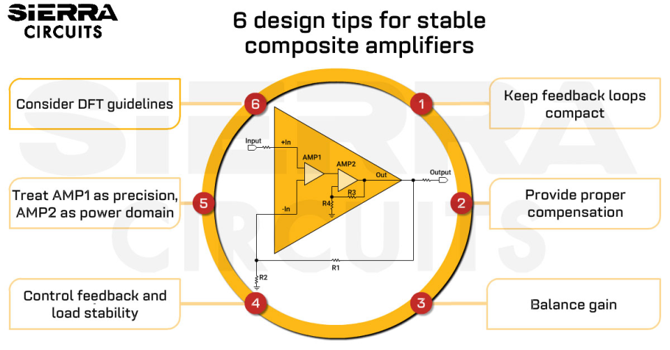
- Signal distortion: Impacts sensitive sensor front-ends, such as op-amp buffers or transimpedance amplifiers in optical sensors. Unintended current paths can reduce signal fidelity, introduce noise, and compromise measurement accuracy or sensor dynamic range. In high-performance designs where a single amplifier cannot meet both noise and bandwidth requirements, composite amplifiers may be considered, though they require careful stability analysis and PCB layout optimization.
- Capacitor voltage ramps: Small leakage or bias currents can slowly charge or discharge capacitors with no direct DC return path. This causes unintended voltage ramps, disrupting timing in circuits like integrators or transimpedance amplifiers.
- Accelerated aging: Degrades materials through electrochemical migration or partial discharge, causing insulation breakdown, corrosion, and leakage paths, which reduce circuit lifespan.
- Lower breakdown strength: Moisture, dust, or tight creepage distances can lower surface breakdown fields, increasing arcing risk. This may lead to component damage, intermittent faults, or safety and reliability issues in high-voltage or compact circuits.
- Safety risks: Compromises safety in critical applications, such as medical, aerospace, or automotive PCBs, where leakage or unintended voltage paths can cause electric shock, arcing, or tracking. This can violate standards like IEC 60601 and endanger users or equipment.
- Errors in high-impedance sources:
- Current-based sources: In photodiodes, leakage diverts current away from the intended node, reducing the measured signal and accuracy.
- Voltage-based sources: In pH electrodes with high series resistance, leakage draws current from the source, causing voltage shifts and measurement errors.
4 design tips to minimize leakage current
Follow these guidelines to minimize leakage current in your boards:
1. Choose laminates with CTI >400 V
- Use laminates with a high comparative tracking index (CTI>400 V). For critical applications such as medical and aerospace, maintain CTI ≥600 V.
| CTI range (V) | Material group | Tracking resistance | Laminates | Design implications |
|---|---|---|---|---|
| ≥600 | Group I | Excellent | Rogers RO4350 B, RO3003 | Allows minimum creepage; ideal for medical, aerospace, and high-voltage precision circuits |
| 400–599 | Group II | Good | Panasonic R-1566(W) | Suitable for most industrial and commercial applications |
| 175–399 | Group IIIa | Moderate | Isola FR408HR, I-Speed, Isola I-Tera MT40, Tachyon-100G | Requires larger creepage for safety; not ideal for high humidity or high-voltage systems |
| 100–174 | Group IIIb | Poor | Nelco N7000-2 | Not recommended for high-voltage or precision designs |
- Select materials with low moisture absorption, such as polyimide laminates, PTFE, or high-grade FR4 instead of standard FR4. For harsh environments, use polymers or laminates designed to resist humidity.
- Use high-quality solder masks and conformal coatings (epoxy, silicone, or parylene) that offer strong insulation and high surface resistivity, even under high voltage.

2. Implement guard rings around high-impedance nodes
- Follow IPC-2221B guidelines for creepage and clearance distances, with derating for humidity, pollution, or altitude.
- Keep high-voltage traces on outer layers instead of inner ones to avoid hidden leakage paths.
- Avoid routing parallel high-voltage traces near sensitive high-impedance nodes.
- Surround high-impedance nodes (e.g., the input of an op-amp, a sensor electrode, or a high-resistance voltage divider) with guard rings biased to the same potential to shunt leakage currents away, which can reduce significant errors, especially in precision analog circuits like pH meters and photodiode amplifiers.

Guard ring on a PCB layout. - Implement guard rings on both sides of the PCB for through-hole components to block leakage paths.
- Use guard planes as an extended form of guard rings for distributed leakage control.
3. Isolate sensitive circuits using Teflon standoffs
- Use non-conductive Teflon standoffs that support the circuit board without providing a path for leakage current.
- Include air wiring to minimize leakage through printed board surfaces for circuits that measure picoamp-level currents.
- Utilize unity-gain buffers to isolate sensitive high-impedance inputs. They draw almost no input current, preventing leakage currents in downstream circuitry from altering the original signal.
4. Include accessible test points for validation
- Have accessible test points on your PCB to simplify insulation resistance (IR) and surface insulation resistance (SIR) tests. These tests help measure leakage under operating voltages and assess the impact of contamination or humidity.
- Make sure there’s adequate creepage and clearance around high-impedance or high-voltage nodes. This allows accelerated stress testing without creating additional leakage paths or overstressing the circuit.
Download our Design for Testing Handbook to learn how to include accurate test points on your layout.

Design for Testing Handbook
7 Chapters - 28 Pages - 45 Minute ReadWhat's Inside:
- PCB testing strategies
- Guidelines to design and place a test point for FPT
- Directives to make your board ICT compatible
- Benefits and drawbacks of various testing methods
- Defects that you can identify through board testing
Download Now
How do manufacturers prevent leakage current in PCBs?
Board manufacturers minimize leakage current by thoroughly cleaning the circuit boards to remove contaminants and applying protective coatings to insulate the circuitry. They also store the finished boards in controlled environments to prevent moisture and dust buildup.
Each of these preventive measures is discussed in detail below:
1. Thorough board cleaning
- Post soldering, the PCB is cleaned with isopropyl alcohol (IPA), rinsed with deionized water, and baked at ~85 °C to remove moisture.
- Ionic residues from flux attract moisture and increase leakage. The manufacturer ensures that flux and cleaning solvents prevent salt formation.
2. Applying protective coatings
- Boards are pre-baked before assembly or coating to drive out absorbed moisture.
- Conformal coatings are applied and properly cured to avoid thin spots or defects that could create leakage paths.
- For extreme environments, additional protective measures such as potting compounds may be applied.
3. Ensuring environmental protection
- Printed boards are stored in hermetically sealed housings to protect against humidity and dust.
- Controlled environments (dry gas purging or desiccants) are used for humidity-sensitive devices.
- Bare or assembled boards are stored in dry cabinets to limit long-term moisture absorption.
Sierra Circuits fabricates and assembles high-quality circuit boards in the United States. Visit our PCB manufacturing capabilities to learn more.
High-leakage current in PCBs is often the result of environmental conditions, material limitations, or design oversights. By choosing appropriate board materials with high CTI and low moisture absorption and following established design standards for creepage and clearance, engineers can significantly reduce leakage current issues and ensure long-term reliability of their electronic systems.
About the technical reviewer:
Dilip Kumar is the Senior Design Manager at Sierra Circuits with over a decade of experience in developing high-speed and HDI PCB designs featuring fine-pitch BGAs. He is proficient in Altium Designer, Cadence Allegro, Eagle PCB, KiCAD, and AutoCAD.
Leading a team of skilled PCB designers and layout engineers, he oversees projects from concept to production, ensuring precision and manufacturability at every stage. Dilip consistently delivers innovative, high-quality designs that meet demanding engineering and business objectives.
Have queries regarding designing high-speed layouts? Post them on our community, SierraConnect. Our design experts will answer them.

About Pooja Mitra : Pooja Mitra is an electronics and communication engineer. With an experience of over three years in the PCB industry, she creates industry-focused articles that help electrical and PCB layout engineers.


Start the discussion at sierraconnect.protoexpress.com