Contents
Perfect PCB soldering is easy! It’s also very rare. What can explain this contradiction? If perfect soldering is easy, why is there so much touchup and rework? The answer, of course, is that it’s easy if you know how. And most of what the soldering “experts” have told us is wrong. The “industry standard” soldering rulebook guarantees failures and high costs.
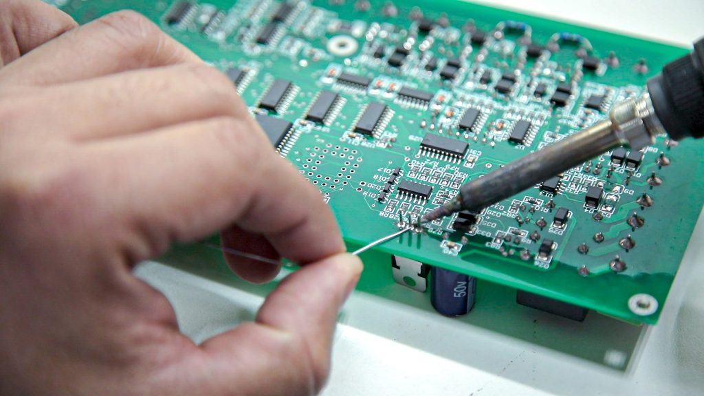
Surprisingly, although soldering is the core process of electronics PCB assembly, few people know how to solder reliably. They often become proficient at hiding defects, but that’s a completely different and unacceptable ability. Visually acceptable connections are not necessarily reliable connections.
The very large amounts of time and money the electronics assembly industry devotes to training and certification have largely been wastes of resources. No one ever learned perfect soldering by attending “industry standard” training.
This and upcoming articles will explain why PCB soldering reliability is so dismal, how we got here, and the necessary corrective actions.
Why we don’t (typically) have perfect PCB soldering
Here’s the problem: Training focuses on the desired appearance of solder rather than how the connection is achieved. And “acceptable” appearance may hide failures in waiting. How the connection was made determines whether the solder connection is reliable and whether catastrophic damage was inflicted on the soldered component.
To produce a visually acceptable connection, the solder will stick to oxides and contaminants at the soldering iron’s temperature. However, the connection lacks an intermetallic bond, and the high temperature degrades bonds inside components.
The altered bonds change electrical values and shorten component life. In just a few seconds of improper application, a soldering iron can shorten the life expectancy of components by decades.
But because the connection looks acceptable and the component damage can’t be seen, the truly dismal state of modern soldering is largely unrecognized.
To learn how to avoid PCB assembly delays and additional costs, download the Design for Assembly Handbook.

PCB Design for Assembly Handbook
6 Chapters - 50 Pages - 70 Minute ReadWhat's Inside:
- Recommended layout for components
- Common PCB assembly defects
- Factors that impact the cost of the PCB assembly, including:
- Component packages
- Board assembly volumes
Download Now
A brief history of PCB soldering procedures
Electronics has not always consisted of solid-state components. For decades before devices like transistors and microprocessors arrived, vacuum tubes represented state-of-the-art. Electrical connections were made by soldering wires to lugs of sockets into which the tubes were inserted. Some of the wires and lugs were quite large and absorbed considerable heat.
Soldering irons were not very efficient at turning electricity into heat. Therefore, the thermal challenge in PCB soldering was preventing the solder from freezing before it completed its flow. So techniques were developed to maximize the amount of heat applied. (Protecting the tubes from heat was not necessary. The tubes were not inserted into the sockets until after soldering. They were never exposed to soldering heat.)
The arrival of solid-state components meant that, for the first time, solder was applied directly to the component rather than wires and sockets. In other words, the components were subjected to the soldering heat. This had profound reliability consequences because heat degraded the component’s electrical properties.
To prevent heat damage during soldering, metal clamps were attached to leads next to the component body. Heat flowed from the soldering iron towards the component but was absorbed by the clamps before reaching the body. The clamps were called “heat sinks,” and they provided absolute protection against heat damage.
Since the dawn of solid-state electronics, every work instruction has called for heat sinks. (See J-STD-001G, Sec. 4.6, for example.) But no one uses heat sinks! How can they? The leads (if there even are leads) are too small. There’s no room to attach a heat sink. But all training programs still tell students to apply heat, like in 1960!
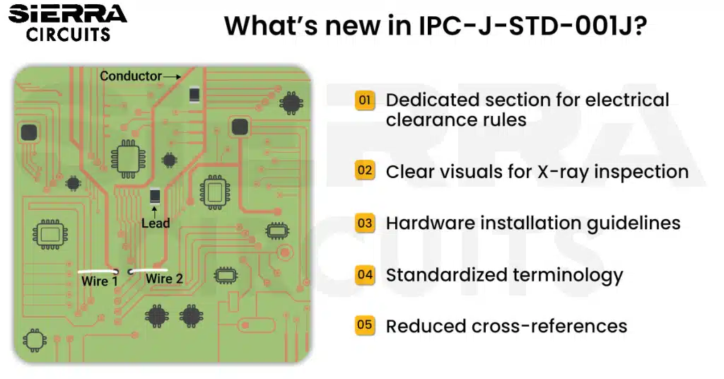
For the latest updates to the IPC-J-STD-001 standard, see what’s new in IPC-J-STD-001J?”
Reflow is not soldering
It gets worse. During the years when soldering procedures were being written, almost all component leads had tin or tin/lead plating. These surfaces melted during “soldering,” and the melted solder simply flowed together with the melted surface metal. Oxides, being lighter than pure metal, floated on top of the liquid metals, where they contacted flux (also lighter than metal) and were eliminated.
Making connections by mixing melted metals is quite easy, but it is not soldering. (The term “reflowing” was often and properly employed.) Soldering is the process of making an intermetallic bond with metal surfaces that do not melt. (They do not “reflow.”) And this requires additional processing steps not needed to mix molten metals. (Sadly, “reflow” continues widespread use even though it is no longer accurate.)
The difference between soldering and reflow (simply mixing melted metals) became very relevant when Europe banned lead in electronics. The transition to a lead-free world focused on the new alloys. Aside from a few quirks, the new solders do not present tremendous problems.
Lead-free solder is less forgiving of a defective process than the traditional tin/lead alloy but performs reasonably well with a properly controlled process. (Since the PCB soldering processes in most companies have been defective, the switch to new alloys was accompanied by difficulties that were wrongly attributed to the solder rather than the process.)
The greater challenge concerns the new lead plating. Tin/lead plating disappeared, of course. But, because of tin whiskers, leads of fewer and fewer components (especially multi-leaded surface mount parts) come with tin surfaces.
These new surfaces do not melt at soldering temperatures. In other words, they must be soldered. But our industry too often sticks to the limited steps that only work for reflow. And the most common training and certification simply guarantee defects and failures.

Soldering is a simple science – If we let it
The reality is that soldering is a science—mostly chemistry but considerable amounts of metallurgy and physics as well. The people who wrote the rule book didn’t approach it that way. They operated based on observation, not realizing that the critical foundations of the science were not obvious.
If they got results that seemed to look right, that’s what they institutionalized. Things need to change if we want a product that works and efficiencies that make profitability possible.
Interestingly, reliability varies inversely with the amount of handling. The most reliable products are produced most efficiently. Our industry has the worst of both worlds – excessive cost and too many failures.
The use of flux
I just said that perfect soldering is easy. But easy doesn’t mean simply slapping melted metal on parts and expecting everything to turn out well. Successful soldering requires knowledge and discipline. And it all starts with solderability.
Solderability is a relatively recent concern in electronics soldering. Until fairly recently, most component leads were plated with tin or tin/lead. Soldering is the process that creates intermetallic bonds with metal surfaces that do not melt during the application of the joining material (solder).
However, tin and tin/lead melt at PCB soldering temperatures, and the solder merely mixes with the melted plating. This is not soldering; it is “reflow” and very easy compared to true soldering.
Reflow is simple
In reflow, there is no need to remove oxides before applying solder; the oxides, being lighter than pure metal, float on the combination of liquid plating metal and liquid solder.
Flux, also lighter than liquid metal, floats on the melted metal, which can easily contact the oxides and break them down. In reflow, the soldering flux simply makes the final connection shiny and cosmetically pleasing.
Most beliefs about soldering originated during this era of reflow. One such belief, which has disastrous consequences today, says that liquid flux should not be used during hand soldering. The belief is that the flux contained in wire solder is sufficient to do the job. While that can be true for reflow, relying exclusively on the flux in solder results in incomplete wetting during soldering.
For an in-depth knowledge of soldering flux, download the Soldering Flex e-book.

Soldering Flux eBook
13 Chapters - 24 Pages - 40 Minute ReadWhat's Inside:
- Why flux is needed
- The ingredients of flux and what they do
- Soldering flux categories
- How to read a flux manufacturer’s technical data
- The best flux for various applications
Download Now
What are the main PCB soldering defects?
The ban on lead in electronics changed our business profoundly by eliminating tin/lead component surfaces. Meanwhile, tin plating has become increasingly uncommon because of concerns about tin whiskers with pure tin. The risk of whisker shorts is quite real for multi-leaded surface mount parts such as I.C.s.
The new component surfaces are not tin or tin/lead; they are metals with higher melting temperatures that do not reflow during the application of the solder. In other words, these are metals that are soldered, not reflowed. And the surfaces must be thoroughly deoxidized before solder is applied.
This will not happen if the flux is contained in the wire solder; the flux in the solder cannot be released until the solder melts. The melted solder forms a barrier between the flux and surface metal, preventing complete deoxidation and causing incomplete wetting.
Liquid Flux is Essential
The only way to ensure that flux reaches the surface oxides before solder melts is by applying liquid flux first. And more than just a trace amount of flux is required. Flux acid (the part that removes oxides) is neutralized during the deoxidation chemical reaction.
Trace amounts of flux will be neutralized before the part has been completely deoxidized. In soldering, flux is more than our friend – it is essential. Yet, every few days, industry “experts” write strongly worded instructions that using liquid flux is a sin.
A widely-used “The Seven Sins of Hand Soldering” video says, “The best way of reducing the use of excessive flux is only to use the flux contained in the solder wire.” (The video is sold by the trade association that publishes standards such as J-STD-001 and A-610. They really should know better.)
Complications
Unfortunately, there’s much more to the flux business than randomly picking an off-the-shelf flux. We’ll look at the science of flux selection next time.
Heat control
The fundamental rules for soldering – the approaches that, in too many cases, continue to be used today – originated about 70 years ago. State-of-the-art electronic components then consisted of vacuum tubes. Soldering was used to connect wires to lugs on sockets into which the tubes were inserted after soldering. All the soldering was performed by hand.
Wires and lugs cannot be damaged by overheating and the sensitive components – the tubes – only entered the picture after soldering was complete. There was a different heat issue, however: some of the wires and lugs were quite large, and the ability of irons to turn electricity into heat was mediocre at best.
Taken together – large pieces of metal and inefficient irons – keeping materials hot enough for the solder to melt and flow well presented significant challenges. To prevent the solder from freezing, training emphasized making parts very, very hot before applying the solder. (The term “cold solder” originated then and was appropriate.
As I will discuss next time, “cold solder” is almost non-existent in modern electronics but shows up frequently, albeit erroneously, as the diagnosis for wetting issues.)
Heat sinks
The arrival of solid-state components (primarily leaded resistors and capacitors in the early days) meant that the active elements of the circuit were exposed to soldering iron heat. An epidemic of component failures followed until the heat-sensitive nature of these new components was recognized.
The solution used metal clamps (“heat sinks”) to protect the component. The clamps were fastened to the lead near the component body. Heat flowed from the iron towards the body but was absorbed (“sunk”) by the clamp. Component failures promptly plummeted.
(Reliability also benefited from machine soldering, which was entirely by wave at the time. Wave soldering and, more recently, surface mount reflow subject components to much lower peak temperatures. Heat damage is primarily a hand soldering issue.)
Soldering small components
Heat sinks provide absolute protection against heat damage but can only be used with components that have leads large enough for clamps to be placed.
The leads of most surface-mount components (even if the components do have leads, which is no longer always the case) don’t fit that description. Using clamps simply isn’t practical now and hasn’t been for at least 25 years.
One of the sorry realities of “industry standard” practices is inertia: once a practice is in place, change happens at a glacial pace (if at all). Consequently, we find requirements like the following from J-STD-001G:
“4.6 Thermal Protection When hand soldering, tinning, or reworking a heat-sensitive component, protective measures shall [D1D2D3] be taken to minimize component heating or prevent thermal shock, e.g., heat sink, thermal shunt, preheat. Protection may be provided through a controlled heating process.”
Failure to conform to the requirement is a defect in all classes of products. Since they don’t have the faintest idea of how to meet the requirement, almost every electronics company is turning out defective products, yet no one seems to care.
What temperature should I solder the PCB?
Heat damage to components is hidden and, as the saying goes, “out of sight, out of mind.” Static damage also occurs inside components and is no more visible than heat damage.
Yet no respectable electronics manufacturing facility would consider operating without rigorous ESD prevention measures. Why the difference? It probably results from market forces. Anti-static requires using hard tools and disposable materials, which adds to enormous sums on a global industry level.
Big revenue supports big advertising budgets, which, in turn, generates universal recognition that static represents a significant reliability hazard. The same applies to moisture.
Heat damage prevention does not involve any material purchases. Since there is no big dollar market, there is no advertising budget, and, hence, limited recognition.
Yes, I overstated the lack of concern about overheating components. Some companies are so concerned about heat that they spend big dollars on soldering irons that maintain a consistent temperature.
Some companies even go so far as to monitor iron temperatures and, if possible, recalibrate once deviation from the set point begins to cause concern. And they’re all wasting money.
Constant temperature irons will cause just as much damage as less precise tools. Heat isn’t controlled by iron temperature; it’s about how iron and solder are used together.
Institutional indifference
During the 1980s, I conducted several soldering workshops for engineers at the Naval Weapons Center Soldering Standards site in China Lake, CA.
“How do you prevent heat damage?” I asked the director (a legendary figure in industry standards who held ultimate authority over all DoD soldering requirements). “Solder quickly,” he said. “And how fast is fast enough?” I replied. Instantly, he declared, “Three seconds.” I was stunned by the lack of science behind the remark. “Three seconds may be fine at times,” I agreed. “But wouldn’t it be too long sometimes and not enough other times?”
In the next class, I demonstrated a technique that ensures component temperature will remain close to the melting temperature of the solder. “I agree that what you are showing works,” the director told me. “But do you expect me to tell the Admiralty we’ve been doing it wrong?” I never returned. And, more than 30 years later, the keepers of standards continue to promote the wrong methods.
For more soldering tips, see 8 soldering tips to watch out for.
Have soldering-related queries? Post them on our forum, SierraConnect. Our experts will resolve them.

Jim Smith
EMSciences
www.emsciences.com