


Contents

On-demand webinar
How Good is My Shield? An Introduction to Transfer Impedance and Shielding Effectiveness
by Karen Burnham
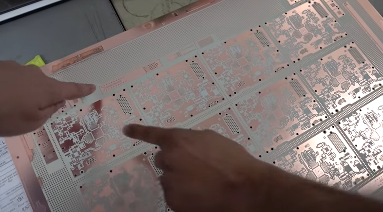
YouTuber and PCB designer Robert Feranec came to visit Sierra Circuits to learn more about our PCB manufacturing and assembly services. As he says in the video, “When you are designing boards, I think it is very useful to know some information about PCB manufacturing.”
Amit Bahl, Sierra’s director of sales and marketing, invited Robert Feranec to show him around and explain to him our manufacturing and assembling process from beginning to end. He was really amazed by several of our techniques, including the drilling part. He learned that layers of PCB can move and shrink, how to get a better value PCB, and many other tips.

The video features:
- The drilling area (3:52)
- The slivers (5:30)
- The teardrops (6:59)
- The etch compensation (10:00)
- The wires (12:39)
- The copper (19:17)
- The thermal relief (20:40)
- 45 and 90 degree angles (21:29)
- The small copper dots (23:19)
- Prepregs, thermal stress and baking PCBs (25:46)
- Drilling (28:15)
- Mask over VIAs (29:48)
- Assembling boards (31:44)
- Minimum distance between two holes (33:03)
- Checking the Gerber files (35:17)
- Plating microvias (36:44)
- The coupons (40:21)
- The price of a PCB (44:00)
PCB Manufacturing – Important facts you should know

Design for Manufacturing Handbook
11 Chapters - 96 Pages - 90 Minute ReadWhat's Inside:
- Annular rings: avoid drill breakouts
- Vias: optimize your design
- Trace width and space: follow the best practices
- Solder mask and silkscreen: get the must-knows
Download Now


