


Contents
On May 17 and 18, Sierra Circuits hosted its first workshop at the Levi’s Stadium. PCB expert Robert Feranec led the two-day training on PCB Board Layout Design Engineering. Watch our video from the event!
SANTA CLARA, CA, MAY 17TH
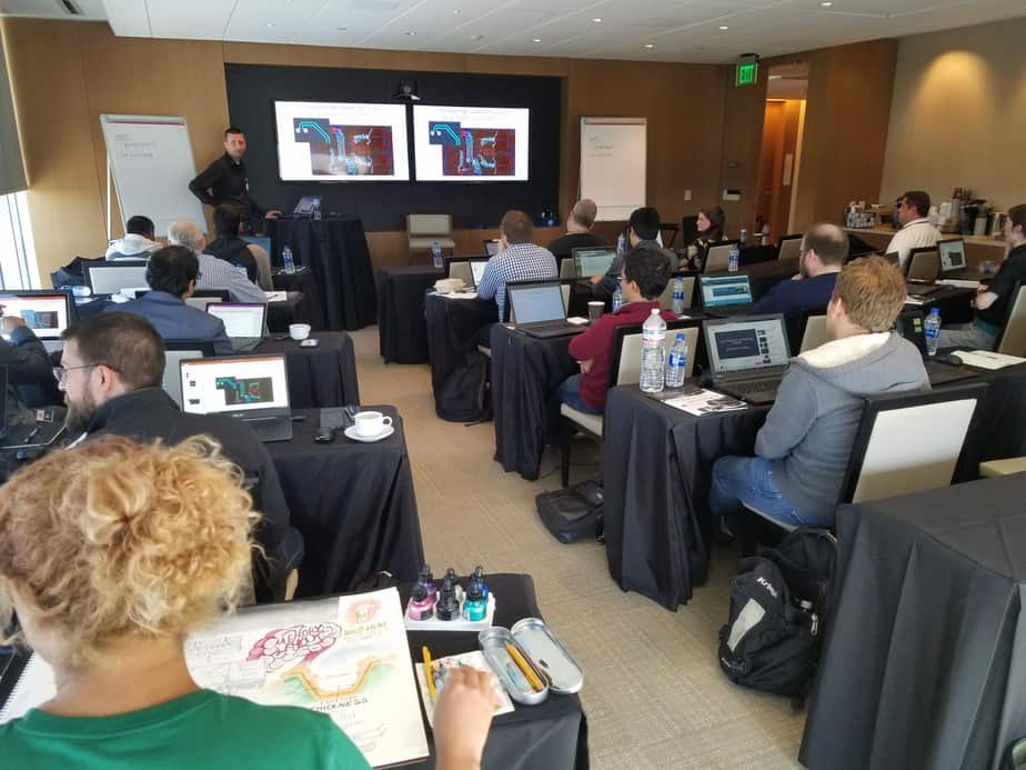
It’s 8:00 AM and the Sierra’s team is running all across the Levi’s Stadium to set up the boardroom for the PCB Board Layout Design Engineering workshop. PCB expert Robert Feranec is uploading his 251-page presentation on the screen of the suite at the 7th floor of the Levi’s. In just a few minutes, he will be sharing his designing knowledge before 25 attendees. This is going to be a two-day intensive training!

Let the workshop begin – crosstalk, routing high-speed signals, differential pair routing, and how to get the right impedance are the first topics covered by Robert. Talking about controlled impedance, he says, “Using an Impedance Calculator is good but you should always communicate with your manufacturer. They will advise you on how to achieve your controlled impedance.”

In the meantime, at the back of the classroom, our super talented Graphic Designer Rachel is drawing two graphics of the workshop. Attendees will try to win them later at our quiz during the cocktail.
Get To Work
As it is stated in the name, a workshop is also meant to make attendees “work”. Robert now gives them an exercise: Calculate the trace width and space for a 100-ohm impedance. The designers get some experience using an impedance calculator which can help them with getting preliminary trace width and space calculations so they can proceed further with their designs. Once a design is almost complete, they can ask the fabrication house to provide the accurate stack-up.

If there is one advice you should follow about DDR2/3 layout, Robert believes it is to not fully route the tracks all at once. Why? “I had a bad experience a few years ago. I used to select groups of pins which I wanted to route and I just fully routed all the connections, Robert explains. It was easy at first but then it just kept getting more complicated. It became impossible to connect the last via and I had to delete half of my design to finish the layout. So now I’m always really careful.” The trick is to do the layout in small parts so you don’t have to start all over again if something goes wrong. Noted.
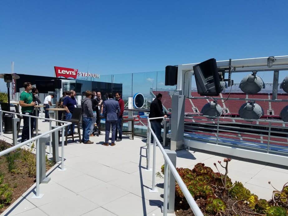
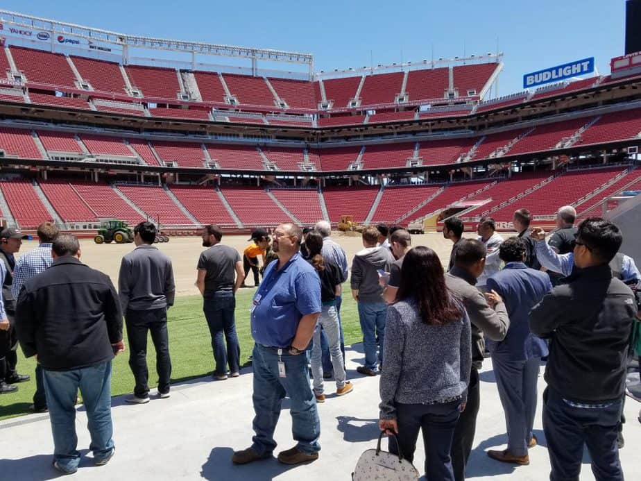
After a private tour of the Levi’s Stadium during the lunch break, it’s already time to go back to class. Attendees are now given a DDR2/3 layout practice with nets to schedule, T-points to add, pin pairs to create, lengths to correct, and traces to route.
MAY 18TH
Robert covers the most common high-speed design rules. Maintain a single-ended and a differential impedance, length match differential pair signals within the pair, keep some space between the “waves”, length match buses and differential pairs, route signal groups using the same topology, be aware of tracks running parallel, use stitching vias when the reference plane changes, and do not do stubs are some of his useful tips.
As we get to the Stack-up part of the workshop, questions just keep on coming from all sides of the boardroom. How many ground solid planes can I use? Can you show us how to order the layers? How to decide on the number of layers? “This is why you should not try to do a stack-up by yourself and always ask your manufacturer for help,” Robert jokes before giving a real explanation.
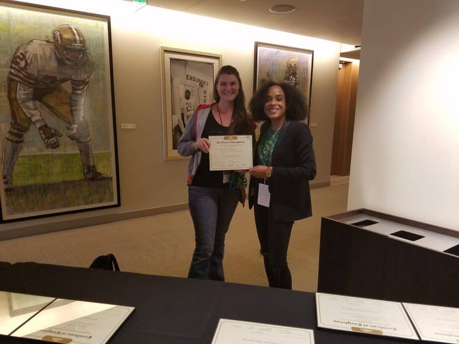
As the two-day layout design training comes to an end, attendees receive their certification signed by Robert. We hope you learned a lot and will join us for our next workshop!
Are you now a master in PCB Board Layout Design Engineering? Take the quiz and find out!


